TSMC is reportedly researching a new substrate design to meet the rapidly growing global demand for processors. From automobiles to mobile devices, PCs to consoles, and even home appliances there is virtually no segment of consumer technology where demand hasn’t increased, that’s only the tip of the iceberg. AI is the new gold mine for both enterprise and consumer technology and chip production is at the center of it all. The demand from chip manufacturers has never been as great as it is now. TSMC is acutely aware of this, especially since AI use is expected to grow a great deal more over the next few years.
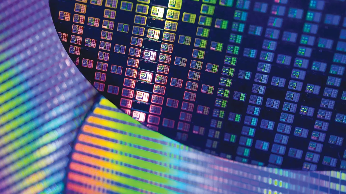
According to a report from Nikkei, which has indicated its sources are people with direct knowledge of the matter, TSMC is working on a new chip packaging design. Presently round wafer substrate designs are used for chip production but according to the report, rectangular substrates are being researched to increase chip yields.
Per Nikkei:
“The idea behind the new approach is to use rectangular panel-like substrates, rather than the conventional round wafers used today, allowing more sets of chips to be placed on each wafer, six people have told Nikkei Asia.”
Research is said to be in its early stages but does show some promise. Sources have said that the new substrate design could allow more than three times the amount of chips to be placed on the wafer than the current round design. It reportedly measures 510 mm x 515 mm (approximately 262,650 sq. millimeters) and the new design could also mean less unused area, and in turn less waste.
However, the idea of a rectangular substrate is not new and has previously been avoided for this type of manufacturing due to increased costs for its use along with imperfection challenges although it is used in the making of PCBs and displays. Other manufacturing/lithography methods could be playing a factor in its potential adoption. Another factor driving the demand for a new design is that increased chip sizes mean less yield per the current round wafer design.
Per Nikkei:
“But as chip size grows to accommodate more transistors and to integrate more memory, the current industry standard — 12-inch wafers with an area of approximately 70,685 sq. millimeters — may not be efficient enough for packaging cutting-edge chips in a couple of years.”
As progressive and exciting as this sounds research is in the early stages and even then, if it comes to pass, implementation is a whole other step. Manufacturing facilities will require extensive overhauling to switch over to a new design which includes updating nearly every aspect of the automated physical process. One source told Nikkei this research is likely part of a long term which could span five to ten years. By then the AI boom could be leveling off but the boon could lay in reduced costs with greater levels of production.
“This shift would require a significant overhaul of facilities, including upgrades to robotic arms, and automated material handling systems to process the different shapes of substrates”
Mark Li – Bernstein Research