Arrow Lake, a new generation of CPUs that Intel originally said would be the first Intel product using Intel 20A tiles, will now be built by external partners and packaged by Intel Foundry, Intel has announced. Intel did not specify who this partner is, but popular speculation would suggest that it is Taiwan Semiconductor Manufacturing Company (TSMC), the semiconductor contract manufacturing and design giant that counts AMD, NVIDIA, and more among its customers.
An Intel VP writes:
- “…Intel 18A in the fab. It’s powered on and booting on operating systems, healthy, and yielding well – and we remain on track for launch in 2025.”
- “One of the benefits of our early success on Intel 18A is that it enables us to shift engineering resources from Intel 20A earlier than expected as we near completion of our five-nodes-in-four-years plan.”
- “With this decision, the Arrow Lake processor family will be built primarily using external partners and packaged by Intel Foundry.”
- “The journey to Intel 18A has been built on the groundwork laid by Intel 20A.”
Intel 18A innovations and applications, per Intel:
- “RibbonFET, Intel Foundry’s implementation of a Gate-all-around (GAA) transistor, improves density and performance versus FinFET.”
- “Optimized ribbon stack delivers superior performance per watt and minimum supply voltage (Vmin).”
- “PowerVia is Intel’s unique industry-first implementation of backside power delivery architecture that improves standard cell utilization by 5-10% and ISO-power performance by up to 4%.”
- “Well-suited for High Performance Computing (HPC) and mobile applications.”
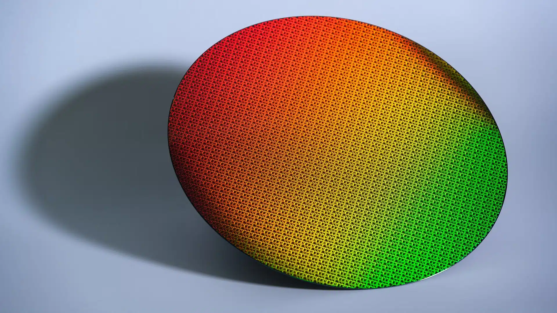
A look at a wafer derived from Intel 18A:
Intel’s Ben Sell added:
[Intel 18A] enabled us to explore and refine new techniques, materials and transistor architectures that are crucial for advancing Moore’s Law. With Intel 20A, we successfully integrated both RibbonFET gate-all-around transistor architecture and PowerVia backside power delivery for the first time, and these learnings have directly informed the first commercial implementation of both technologies in Intel 18A. This points to the iterative nature of semiconductor innovation, and we’re excited to bring these advancements to all Intel Foundry customers.
Focusing resources on Intel 18A also helps us optimize our engineering investments. When we set out to build Intel 20A, we anticipated lessons learned on Intel 20A yield quality would be part of the bridge to Intel 18A. But with current Intel 18A defect density already at D0
Join the discussion in The FPS Review Forums...
Discussion
Join Discussion →No replies yet. Be the first to reply on the forum.
Discussion
Join Discussion →No replies yet. Be the first to reply on the forum.