
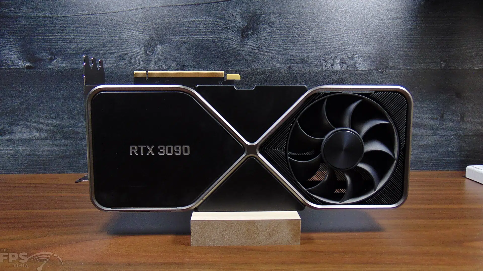


The GeForce RTX 3090 is based on the Ampere architecture and manufactured on Samsung 8nm; it uses the GA102-300 die. It has 2nd Generation RT Cores and 3rd Generation Tensor Cores supporting Ray Tracing and NVIDIA DLSS. The GeForce RTX 3090 has 82 SMs, 10,496 CUDA Cores, 328 TMUs, 112 ROPs, 82 RT Cores (2nd Gen), and 328 Tensor Cores (3rd Gen.) It operates with a boost clock of 1695MHz. It has 24 GB of GDDR6X memory on a 384-bit bus at 19.5GHz providing 935.8GB/s of memory bandwidth. The TDP/TBP is 350W.
NVIDIA GeForce RTX 3090 GPU Family Specifications
| GPU Family Basics | |
|---|---|
| GPU Manufacturer | NVIDIA |
| GPU Generation | RTX 30 Series |
| GPU Architecture Name | Ampere |
| GPU Die Code | GA102-300 |
| Default TGP | 349 W |
| GPU Family Memory | |
|---|---|
| Default Memory Bandwidth | 0.936 GHz |
| Default Memory Size | 24 GB |
| Memory Bus Width | 384 bit |
| Memory Type | GDDR6X |
| GPU Family Chip Details | |
|---|---|
| Transistors | 28.3 |
| Die Size | 628 mm^2 |
| CUDA Cores | 10496 |
| RT Cores | 82 |
| ROPs | 112 |
| TMUs | 328 |
| GPU Family Clock Speeds | |
|---|---|
| Default GPU Base Clock | 1395 MHz |
| Default GPU Boost Clock | 1695 MHz |
| Default Memory Clock | 19.5 GHz |