NVIDIA GeForce RTX 4070 Ti SUPER GPU Family Specifications

We reviewed the ASUS TUF Gaming GeForce RTX 4070 Ti SUPER, which offers more performance and VRAM than the GeForce RTX 4070 Ti, replacing it at the same price point. This is a good value, and a value improvement considering you are getting more performance and VRAM at the same price. It faces fierce competition in this space, but offers a compelling list of features like DLSS, and RTX features as well as better Ray Tracing performance. It's built well, runs very cool and power efficient, providing value at this price segment.

GPU Family Basics
GPU Manufacturer NVIDIA
GPU Generation RTX 40 Series
GPU Architecture Name Ada Lovelace
GPU Die Code AD100
Default TGP 285 W
Launch Price $799
GPU Family Memory
Default Memory Bandwidth 672 GB/s
Default Memory Size 16 GB
Memory Bus Width 256 bit
Memory Type GDDR6X
GPU Family Chip Details
Transistors
Die Size
CUDA Cores 8448
RT Cores 66
ROPs 96
TMUs 264
GPU Family Clock Speeds
Default GPU Base Clock 2340 MHz
Default GPU Boost Clock 2610 MHz
Default Memory Clock 21 GHz

Notably, the GeForce RTX 4070 Ti SUPER is now based on the AD103 die, which is the GeForce RTX 4080 cut-down, whereas previously the GeForce RTX 4070 Ti was the AD104 die. This gives the GeForce RTX 4070 Ti more options, namely core increases and notably VRAM capacity increase and memory bus width increase with bandwidth increase. We see the CUDA Cores increasing by 10%, but with that is more Tensor Cores, more RT Cores, more TMUs, and 20% more ROPs. We also find that the boost clock is the same, however the base clock gets a small increase. 

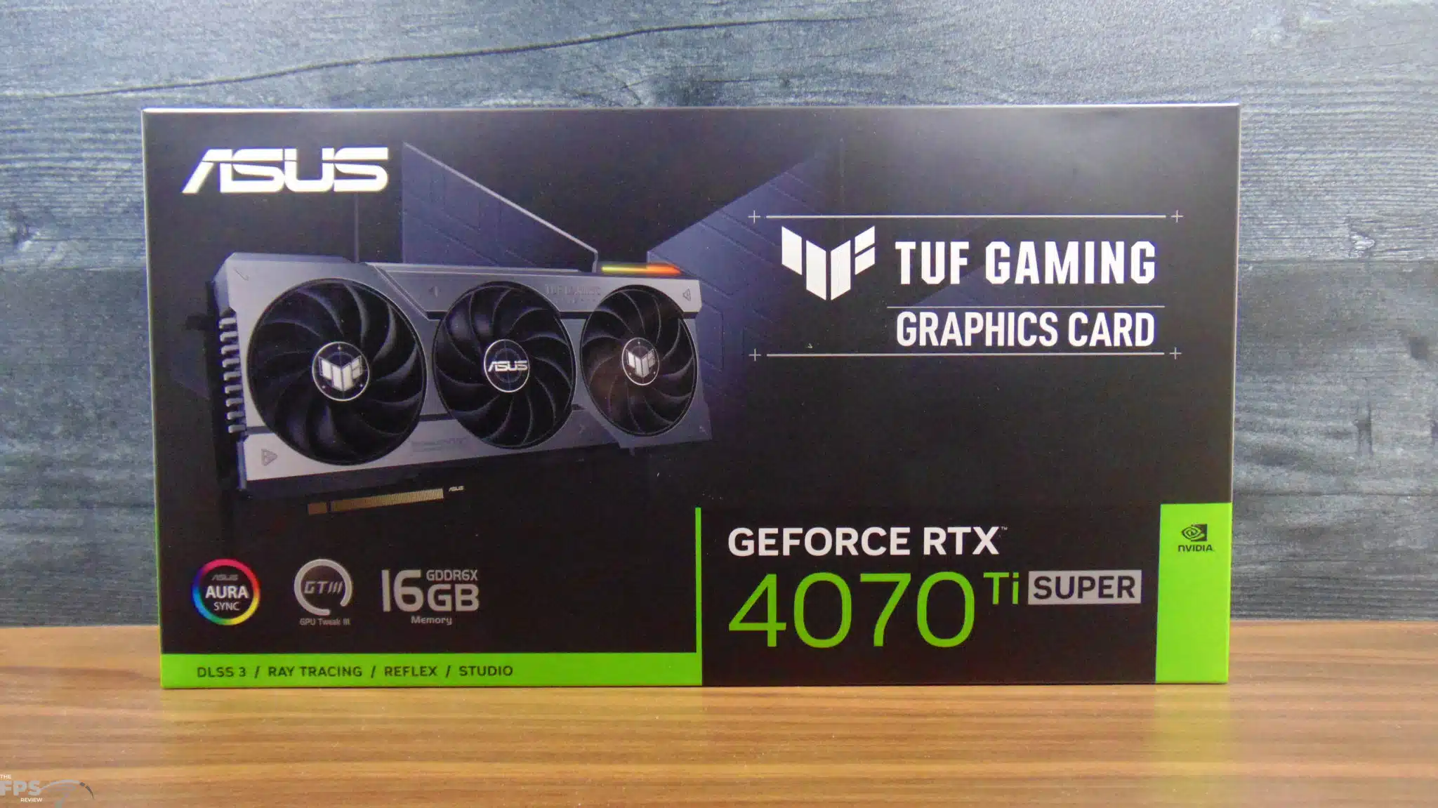
The other big part here is that the bus width increases from 192-bit to 256-bit, which allows the video card to have 16GB of VRAM now instead of 12GB. With the memory bus width increase, bandwidth increases by 33%. Incredibly, the TDP stays the same at 285W. Remember, you are getting all of this at the same $799 price point the GeForce RTX 4070 Ti was at.