
Taiwan Semiconductor Manufacturing Company, or TSMC, has partnered with another giant in the semiconductor sector. They and American semiconductor manufacturing company, Broadcom Inc., have created another world’s first. They’ve created the world’s first 2x reticle size interposer to enhance the CoWoS platform. CoWoS® , or Chip-on-Wafer-Substrate, is TSMC’s approach for integrating logic computing and memory into a 3-D stacked chip design. TSMC has accomplished multiple records with this design since 2012.
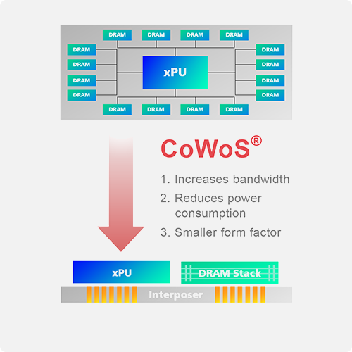
This new interposer technology is currently stated as being the world’s largest at around 1,700mm2. It will allow for more SoCs and is compatible with TSMC’s new 5 nm, or N5, fabrication node. In enhancing their CoWoS technology it can now accomodate up to 96GB of HBM memory. In turn that HBM can operate up to 2.7 terabytes per second which is almost 3 times what they achieved four years ago. HPC Systems as well as ASIC’s will see a large performance increase with this new design as it yields increases computing power.
From TSMC’s news post,
“In this TSMC and Broadcom CoWoS platform collaboration, Broadcom defined the complex top-die, interposer and HBM configuration while TSMC developed the robust manufacturing process to maximize yield and performance and meet the unique challenges of the 2X reticle size interposer.”
3-D stacking, interposers, chiplets, are all terms becoming increasingly more common in modern day technological vernacular. The concepts are not new but they are being implemented in new ways from every sector of processor manufacturing. In the last few weeks many stories have come forward about them. The reasoning for these approaches is to increase computing power while maintaining costs. As we continue to see node processes shrink dies this allows for dies to be stacked instead of multiple placements on the PCB as has been the norm for many years. Interesting factoid, TSMC was the world’s first dedicated semiconductor foundry and was established in 1987.