
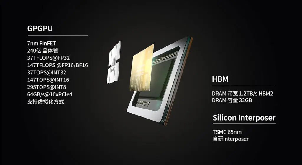
Tianshu Zhixin has revealed that Big Island, China’s first 7-nanometer GPU, is about to enter mass production and commercial delivery. The company claims that the GPU is capable of offering nearly twice the performance of mainstream manufacturers’ products at a lower power consumption, which seems impressive since it only uses half the chip area of similar products. Big Island features a 32 GB HBM2 memory configuration and a peak FP32 rate of 37 TFLOPS.
| GPU Name | AMD Instinct MI100 | NVIDIA A100 | Big Island |
|---|---|---|---|
| Process Node | TSMC 7nm | TSMC 7nm | TSMC 7nm |
| Architecture | CDNA 1 | Ampere | Unknown |
| Transistors | 50 Billion | 54 Billion | 24 Billion |
| Cores | 7680 | 6912 | TBC |
| Memory | 32 GB HBM2 | 40 GB HBM2 | 32 GB HBM2 |
| Memory Bandwidth | 1.2 TB/s | 1.6 TB/s | 1.2 TB/s |
| FP32 Compute | 23.1 TFLOPs 46.1 TFLOPs (Matrix) | 19.5 TFLOPs 156 TFLOPs (Tensor) 312 TFLOPs (sparsity) | 37 TFLOPs |
| BFLOAT16 Compute | 92.3 TFLOPs | 312 TFLOPs 624 TFLOPs (sparsity) | 147 TFLOPs |
| TDP | 300W | 400W | 300W |
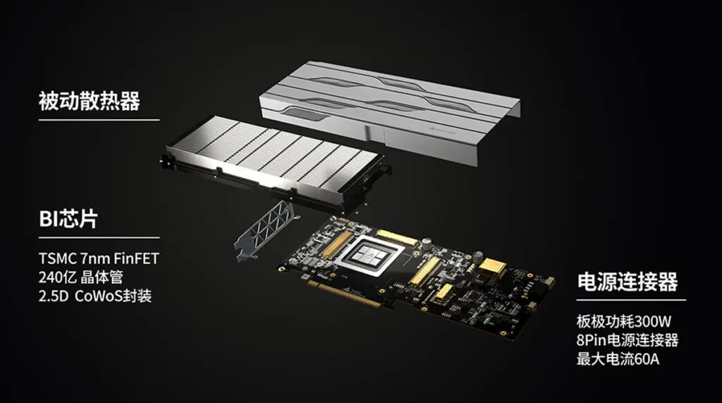
As the first flagship product launched by Tianshu Zhixin, BI is the first fully self-developed GPGPU cloud high-end training chip based on the universal GPU architecture. It adopts the industry-leading 7nm manufacturing process, 2.5D CoWoS package, and accommodates 24 billion. Transistor, supports FP32, FP/BF16, INT32/16/8 and other multi-precision data mixed training, integrated 32GB HBM2 memory, storage bandwidth up to 1.2TB, single core can perform 147 trillion FP16 calculations per second (147TFLOPS@FP16)
Sources: Tianshu Zhixin, Wccftech