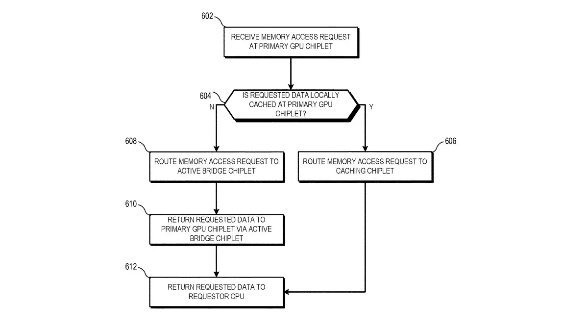
AMD has filed a patent for an active bridge chiplet with integrated cache that would allow partitioning of smaller-group SoC chiplets, improving communication among them by providing high-bandwidth die-to-die interconnectivity. The chiplets would access the memory cache via a single registry instead of individual channels; no software-specific implementation would be needed. AMD presently uses an L3 cache called Infinity Cache for its RDNA 2 architecture. This new design could help alleviate issues with the functioning of multiple GPU dies seen as one device by the CPU and applications.
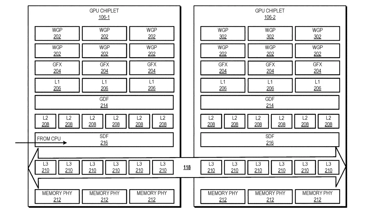
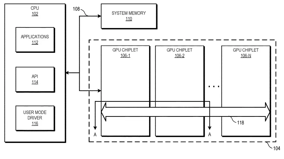
Currently, various architectures already have at least one level of cache (e.g., L3 or other last level cache (LLC)) that is coherent across the entire conventional GPU die. Here, the chiplet-based GPU architecture positions those physical resources (e.g., LLC) on different dies and communicably couples those physical resources such that the LLC level is unified and remains cache coherent across all GPU chiplets. Thus, although operating in a massively parallel environment, the L3 cache level is coherent.
Sources: Free Patents Online, VideoCardz