SK hynix has announced the development of HBM3. At 819 GB/s, it is the fastest DRAM in the world. It is 78 percent faster than HBM2E. The base silicon is shaved down to 30 micrometers and has 12 chips layered onto it. The new memory features on-die error correction and comes in two sizes, 16 GB and 24 GB, and are expected to be used in datacenters, machine learning applications, and supercomputing sectors. Considering how high-end graphics cards have been adopting similar memory capacities, GPU manufacturers may take the new DRAM into consideration for future products. AMD has already used HBM2 for some of its consumer graphics card offerings.
Press Release:
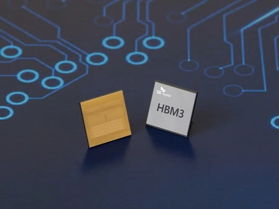
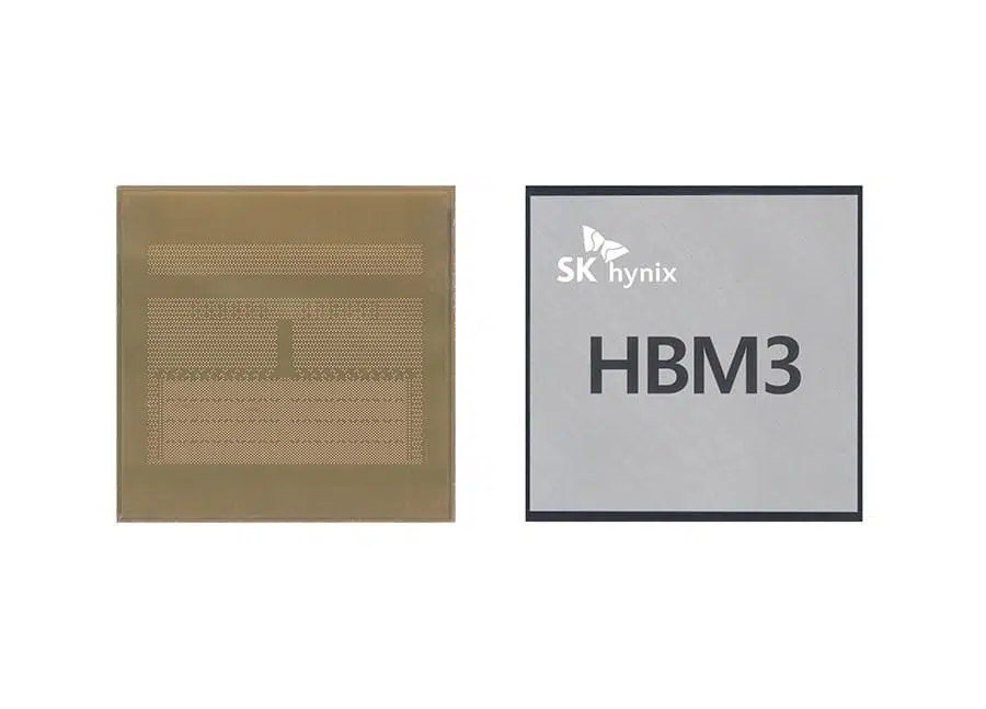
SK hynix Inc. (or “the Company”, www.skhynix.com) announced that it has become the first in the industry to successfully develop the High Bandwidth Memory 3, the world’s best-performing DRAM.
HBM3, the fourth generation of the HBM technology* with a combination of multiple DRAM chips vertically connected, is a high-value product that innovatively raises the data processing rate.
*Previous three generations are HBM, HBM2, and HBM2E, which is an update to the HBM2 specification with increased bandwidth and capacities.
The latest development, which follows the start of mass production of HBM2E in July last year, is expected to help consolidate the company’s leadership in the market. SK hynix was also the first in the industry to start mass production of HBM2E.
SK hynix’s HBM3 is not only the fastest DRAM in the world but also comes with the biggest capacity and significantly improved level of quality.
The latest product can process up to 819GB (Gigabyte) per second, meaning that 163 FHD (full-HD) movies (5GB each) can be transmitted in a single second. This represents a 78% increase in the data-processing speed compared with the HBM2E.
It also corrects data (bit) errors with the help of the built-in on-die error-correction code, significantly improving the reliability of the product.
SK hynix’s HBM3 will be provided in two capacity types of 24GB – the industry’s biggest — and 16GB. For the 24GB product, SK hynix engineers ground the height of a DRAM chip to approximately 30 micrometers (μm, 10-6m), equivalent to a third of an A4 paper’s thickness, before vertically stacking 12 chips using the through silicon via technology.
*Through Silicon Via (TSV): An interconnecting technology that links the upper and lower chips with an electrode that vertically passes through thousands of fine holes on DRAM chips
HBM3 is expected to be mainly adopted by high-performance data centers as well as machine learning platforms that enhance the level of artificial intelligence and supercomputing performance used to conduct climate change analysis and drug development.
“Since its launch of the world’s first HBM DRAM, SK hynix has succeeded in developing the industry’s first HBM3 after leading the HBM2E market,” said Seon-yong Cha, Executive Vice President in charge of the DRAM development. “We will continue our efforts to solidify our leadership in the premium memory market and help boost the values of our customers by providing products that are in line with the ESG management standards.”
Source: SK hynix (via PR Newswire)