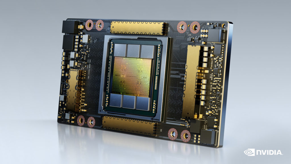
Known leaker @kopite7kimi has posted that the NVIDIA GH100 “Hopper” GPU could turn out to be a huge monolithic designed die at “slightly less than 1000 mm².” Another known leaker, @Greymon55, also chimed in to say that it will be a single die. The reason behind both stating a monolithic architecture came from a previous post in 2019 by @kopite7kimi that NVIDIA could switch over to an MCM design with Hopper.
DO NOT overreact. We know the actual die size will be significantly smaller than the package size.
— kopite7kimi (@kopite7kimi) January 29, 2022
But GH100>GA100 is confirmed. 😁
GH100 does not have MCM, it’s still monolithic.
— Greymon55 (@greymon55) January 29, 2022
The confusion over whether or not Hopper would utilize an MCM design also stemmed from an April Fools’ joke in 2021. NVIDIA released an image of an H100 package featuring two dies comprising “43008 CUDA Cores across 336 SMs coupled to 48 GBs of HBM4 Memory.” Since AMD has used MCM designs with multiple generations of products, it seemed plausible that NVIDIA could do the same for a future graphics card.

The claim of GH100 being around 1000 mm² is possible, but numerous people have commented that the reticle size for i193 and EUV lithography used in producing current dies has a maximum size limit of 858 mm2. Although technically that is slightly less than 1000mm², the current Ampere GA100 die is “currently the world’s largest 7 nm die with an area of 826 mm2,” which means that if this rumor is to be taken on a more literal scale, then NVIDIA would have to employ some customized means of manufacturing for such a larger-sized die.
entirely possible they are using a special etching /reticle machine for it.
— 𒐪𒐪𒐪𒐪𒐪𒐪𒐪𒐪𒐪John Smith𒐪𒐪𒐪𒐪𒐪𒐪𒐪𒐪𒐪 (@400404o4) January 29, 2022
but yeah maybe its exactly 858mm² – the current limit
Sources: VideoCardz, Wccftech, Notebookcheck