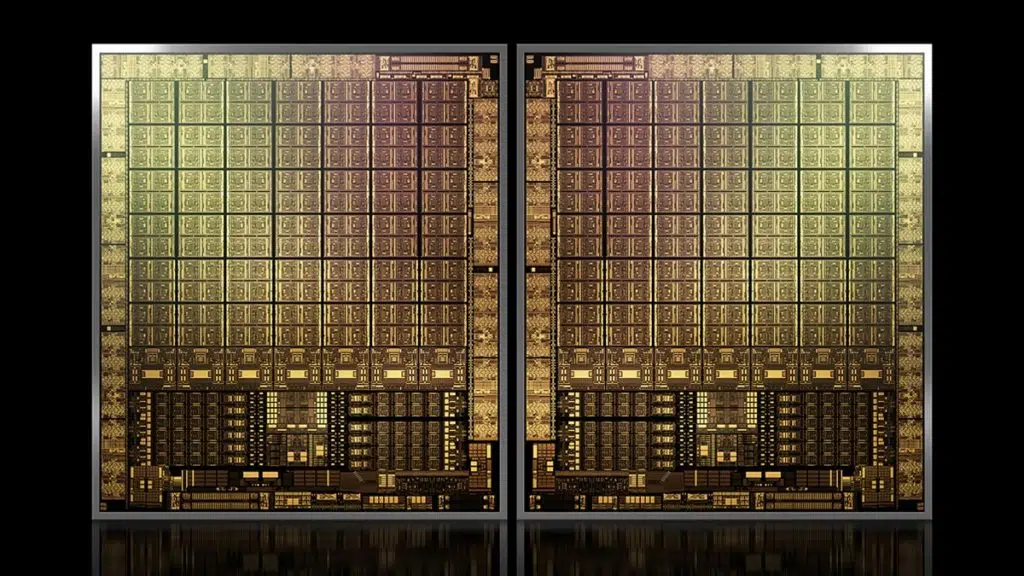
NVIDIA’s next-generation, flagship data center “Hopper” GPU, the GH100, is going to a have a pretty mind-blowing specifications sheet, according to new rumors originating from Chip Hell. As teased by user zhangzhonghao, this GPU will supposedly boast a transistor count of 140 billion, an incredible number that puts current flagship data center GPUs such as AMD’s Aldebaran (58.2 billion transistors) and NVIDIA’s GA100 (54.2 billion transistors) to shame. Previous reports have indicated that NVIDIA’s GH100 will be manufactured on a 5-nanometer process and feature a die size of nearly 1000 mm2, making it the biggest GPU ever made.
NVIDIA Hopper GH100 GPU Rumored To House Over 140 Billion Transistors In A Massive 5nm Package (Wccftech)
- In terms of density, the NVIDIA Ampere A100 amounts to 65.6M transistors per mm2, while the Aldebaran GPU (based on its speculated die size of 790mm2) should have a density of 73.6M transistors per mm2.
- Assuming that the GH100 measures around 900mm2, its density should easily cross 150M transistors per mm2. That’s more than twice the density increase on the 5nm process node.
- We can’t give a rundown on the core count yet since we don’t know the number of cores featured in each SMs but if it’s going to stick to 64 cores per SM, then we get 18,432 cores which are 2.25x more than the full GA100 GPU configuration.