Introduction
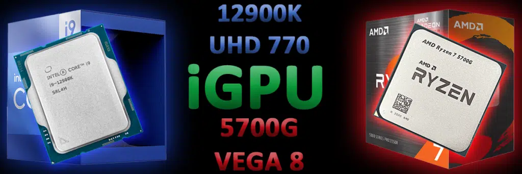
The fight of 2022 is here in the integrated graphics CPU space, Intel Alder Lake versus AMD Cezanne, AMD and Intel integrated graphics performance, two CPUs with integrated graphics fight it out to see who offers the best value in gaming without a dedicated video card. We have taken the best and fastest integrated graphics from both camps to put them head-to-head to compare gaming performance and compute performance.
From Intel, we have the Intel Core i9-12900K CPU with Intel UHD Graphics 770 iGPU GFX onboard. From AMD we have the AMD Ryzen 7 5700G APU with AMD Radeon Graphics in the form of AMD Radeon RX Vega 8 onboard. How good can you game without a dedicated video card on the fastest integrated graphics desktop CPU and desktop APU in 2022? That is what we will find out.
Intel UHD Graphics 770 vs AMD Radeon RX Vega 8 Specifications
Before we dive into each integrated graphics specifically, we are going to put both in a table to show the main differences, best we can. Intel and AMD define their architectures and configurations differently, so what is considered a “Shader Core” or an “Execution Unit” are all different, and architectures cannot be directly compared, but we will do our best to line up what makes sense for comparison below. This will give you an overall idea of what separates them on a hardware level.
| Specification | Intel UHD Graphics 770 (12900K) | AMD Radeon RX Vega 8 (5700G) |
|---|---|---|
| Architecture Name | Intel Xe LP | Alder Lake GT1 | Gen 12.2 | GCN 5.0 | Vega Raven Ridge | Vega 8 |
| Execution Units/CUs | 32 | 8 |
| “Shader Units/Cores” | 256 | 512 |
| ROPs | 8 | 8 |
| TMUs | 16 | 32 |
| GPU Frequency | 1550MHz | 2000MHz |
| Pixel Fillrate | 12.4 GPixel/s | 16 GPixels/s |
| Texture Fillrate | 24.8 GTexel/s | 64 GTexel/s |
| DirectX Feature Level | 12.1 | 12.1 |
| Shader Model | 6.6 | 6.6 |
| OpenCL | OpenCL 3.0 | OpenCL 2.1 |
| Vulkan | 1.2.203 | 1.3.203 |
| Hardware Encoder | Intel QuickSync Version 8 (QSV) | AMD VCN 2.2 |
Intel Core i9-12900K UHD Graphics 770
Both of the CPUs we are testing today are new kids on the block, as they were both recently released. Let’s go over the 12th Gen Intel Core Desktop Processor first with the Intel Core i9-12900K CPU. The 12900K is codenamed Alder Lake-S 881 with an SSPEC of SRL4H. This is a hybrid CPU architecture on the socket V LGA1700 Intel platform launched at the end of October 2021 based on the Intel 7 manufacturing process. The launch RCP Pricing USD 1K is $589 for this CPU.
Uniquely this CPU brings a new design architecture, called a hybrid architecture that marries Performance Cores (P-core) and Efficiency Cores (E-core) together into a combined design. The P-cores support Intel Hyperthreading. You can read about the architecture in our initial review. The Intel Core i9-12900K is made up of 8 P-cores and 8 E-cores. This means it has a total of 16 “cores” and a total of 24 threads. The Intel Turbo Boost Max 3.0 frequency is 5.2GHz, the P-Core Max Turbo is 5.1GHz and the E-Core Max Turbo is 3.9GHz. The base power is 125W and the Max Turbo Power is 241W.
Intel UHD Graphics 770


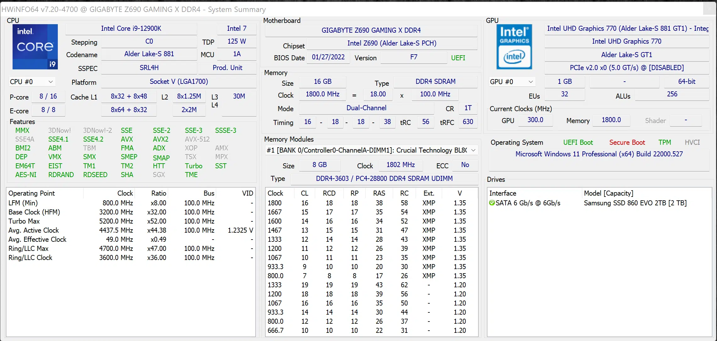
We have reviewed this CPU for its CPU performance, but today is the first time we are focused purely on its integrated graphics (iGPU) performance. The CPU utilizes the Intel UHD Graphics 770 onboard. The Intel UHD Graphics 770 is based on Intel’s Xe LP Architecture of the 12th Generation called Gen12 for Alder Lake-S, formerly called 10ESF. Though the UHD 770 in Alder Lake actually goes slightly beyond that and is based on the Generation 12.2 architecture, versus the 12.1 architecture in Rocket Lake CPUs.
The LP in the architecture name stands for low power and that means this is the low power variant of the Intel Xe GPU architecture, 15W TDP in the 12900K. The Intel Xe GPU architecture should not be confused with Intel’s upcoming dedicated GPU line known as Alchemist, which is a completely new and different beast. The Intel Xe GPU architecture is related to Intel’s Iris Xe Graphics in the mobile space.
There are some new abilities added in the current Generation 12.2 Alder Lake version of the Intel Xe architecture, such as Sampler Feedback, Dual Queue Support, DirectX 12 View Instancing Tier2, and AV1 8-bit and 10-bit fixed-function hardware decoding. It also supports Variable Rate Shading Tier 1. The Intel UHD Graphics 770 is the top-end variant on Alder Lake CPUs, there is a UHD 730 and UHD 710 versions available, but those are on the earlier Rocket Lake Gen 12.1 architecture. The 12900K, 12700K, and 12600K use the newer Generation 12.2 architecture, and the 12900K itself has the fastest clock speed implementation of the UHD 770.
The Intel UHD Graphics 770 is naturally also manufactured on the Intel 7 process. The UHD 770 is made up of 32 Execution units and 256 Shading units as Intel defines them. It has a max boost clock in the range of 1450-1550MHz, on the 12900K the boost is the full 1550MHz and this is the highest it will boost at. It has 8 ROPs but only 16 Texture Mapping Units, therefore its texture fillrate is a bit low, and the pixel fillrate is low because of the lower frequency. The architecture does work with AMD FidelityFX Super Resolution (FSR) technology, though it isn’t optimized for it, it works, to varying degrees since FSR doesn’t require vendor support.
One good thing it has going for it is the inclusion of Intel’s latest Version 8 QuickSync hardware decoder/encoder. It adds VP9 12-bit and 12-bit 4:4:4 hardware decoding and HEVC 12-bit 4:2:0, 4:2:2, and 4:4:4 hardware decoding. It also fully supports AV1 decoding. The encoding performance is actually very good, industry-leading in fact. From a software side, it supports DirectX 12.1 and Shader Model 6.6 and is also using OpenCL 3.0.


AMD Ryzen 7 5700G Radeon RX Vega 8
The next kid on the block is the new AMD Ryzen 7 5700G APU, which is also a recent release. Like the 12900K, it has integrated graphics that are simply called AMD Radeon Graphics. The AMD Ryzen 7 5700G is a traditional designed CPU utilizing AMD’s current latest architecture, Zen 3. The Ryzen 7 5700G is codenamed Cezanne on the AM4 platform. This APU was announced in the spring of 2021, and AMD finally made it available for the consumer to purchase later that year. The APU is based on the TSMC N7 node and the MSRP at launch was $359.
Being a traditional CPU the AMD Ryzen 7 5700G is an 8 Core/16 Thread CPU, similar to the Ryzen 7 5800X. In fact, it has a lot of things in common with the Ryzen 7 5800X, just think of it as a step down from a 5800X, but with AMD Radeon Graphics integrated onboard. The maximum turbo or boost clock on this CPU is up to 4.6GHz. The TDP is 65W.
The CPU itself is made on the latest Zen 3 architecture, so it carries over all the features of the AMD Ryzen 5000 series CPUs inherent to them, including the CCD and CCX layouts. However, there is one major difference, the Ryzen 7 5700G only supports PCI-Express Gen 3.0, not 4.0. This won’t make a difference for the integrated graphics performance, or CPU performance.
AMD Radeon RX Vega 8 (5000 Series Variant)


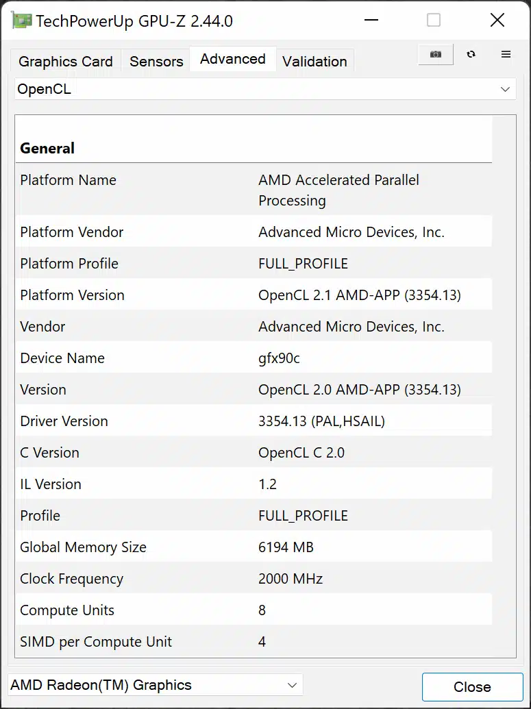

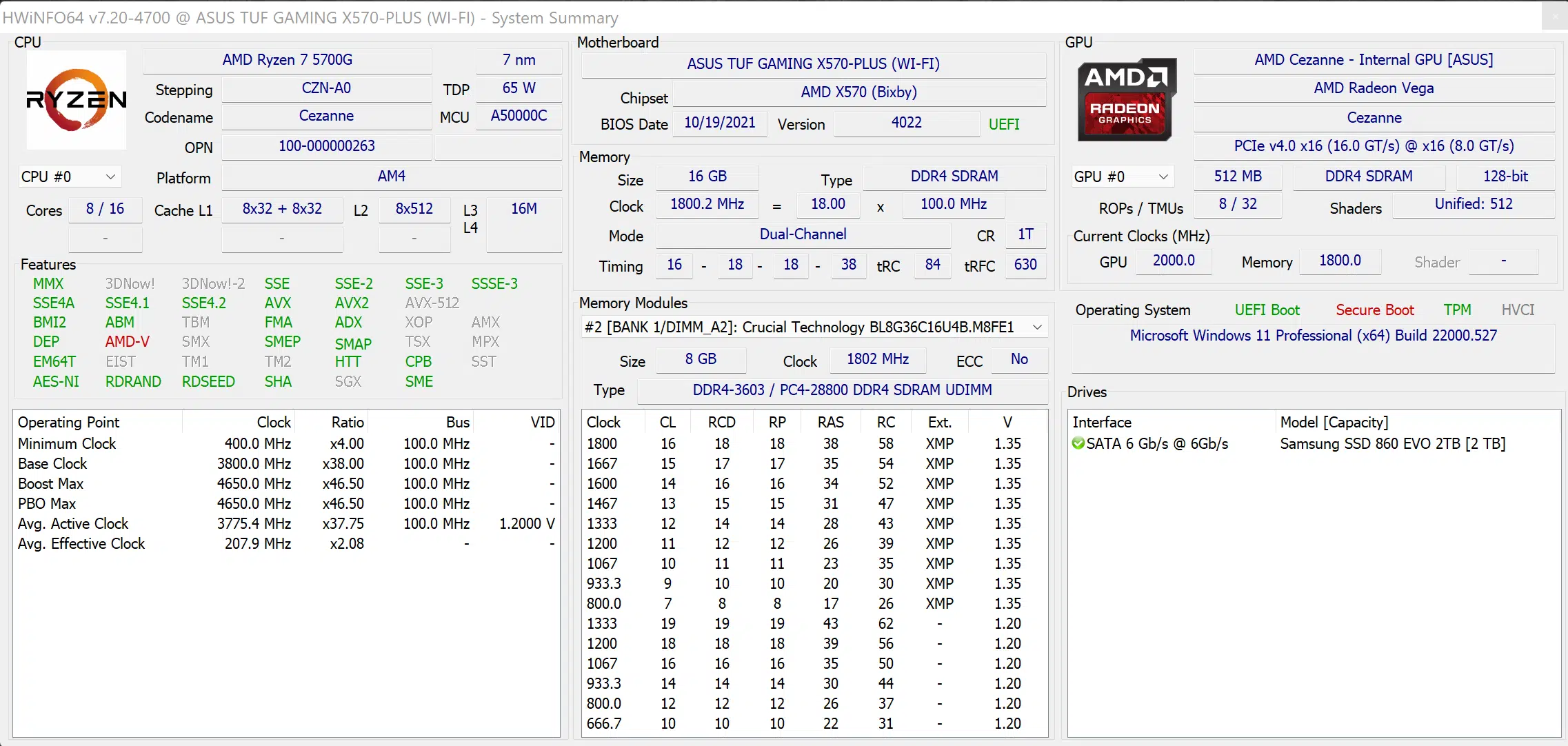
Onboard the AMD Ryzen 7 5700G is the AMD Radeon RX Vega 8 Radeon Vega Graphics. The AMD Ryzen 7 5700G, unfortunately, does not use the newer RDNA or even RDNA2 architecture. Instead, it is using the previous generation to RDNA which is quite aged now. We are talking all the way back to the Graphics Core Next (GCN) architecture, specifically GCN 5th Generation or GCN 5.0. Radeon RX Vega 8 is based on the Raven Ridge Vega generation, which unfortunately dates back to 2017.
As the name suggests, AMD Radeon RX Vega 8 is made from 8 Compute Units giving it 512 Streaming Processors or shader cores. It has 8 ROPs and 32 Texture Mapping Units. On the Ryzen 7 5700G the Vega 8 Graphics is clocked at a high 2000MHz (2GHz) clock speed. This gives us a good pixel and texture fillrate number, much greater than the Intel UHD Graphics 770. The architecture does not support Ray Tracing, and it also does not support Variable Rate Shading at all, whereas the Intel UHD Graphics 770 does support Tier1 VRS. It does however work just fine with AMD FidelityFX Super Resolution (FSR) technology.
AMD Radeon RX Vega 8 utilizes Video Core Next (VCN) version 2.2. This is actually a step-up from NAVI/RDNA1 which used VCN 2.0. However, it is nowhere near the latest version of VCN which with RDNA2 is VCN 3.0+. VCN 2.2 on Vega 8 does not support AVI1 decoding, so Intel UHD Graphics 770 has a leg-up in that department.
From a software perspective, the Radeon RX Vega 8 supports DirectX 12.1 and Shader Model 6.6. Interestingly, it does only support OpenCL 2.1 at this time, even with the latest drivers installed OpenCL 2.1 is all we had available to us, therefor the Intel Graphics UHD 770 does support OpenCL 3.0 right now, which you will see in our compute tests makes a difference. The Vulkan version, however, is higher with Vega 8 versus UHD 770.
Both integrated graphics options naturally utilize the system memory size and bandwidth as their primary memory source. Therefore whatever size RAM you have installed, and the frequency it runs at, is the available bandwidth these graphics cores have to utilize, it’s all system dependent.

