Samsung has revealed that it is targeting mass production of 2 nm process technology by 2025 and 1.4 nm by 2027. The company shared the news during this week’s Samsung Foundry Forum 2022 event, in which it also announced plans to expand the production capacity for the advanced nodes by more than 3X by 2027. Non-mobile applications, including HPC and automotive, are also expected to exceed 50% of Samsung’s foundry portfolio by 2027.
“The technology development goal down to 1.4nm and foundry platforms specialized for each application, together with stable supply through consistent investment are all part of Samsung’s strategies to secure customers’ trust and support their success,” said Dr. Si-young Choi, president and head of Foundry Business at Samsung Electronics. “Realizing every customer’s innovations with our partners has been at the core of our foundry service.”
From Samsung Newsroom:
Samsung Electronics, a world leader in advanced semiconductor technology, announced today a strengthened business strategy for its Foundry Business with the introduction of cutting-edge technologies at its annual Samsung Foundry Forum event.
With significant market growth in high-performance computing (HPC), artificial intelligence (AI), 5/6G connectivity and automotive applications, demand for advanced semiconductors has increased dramatically, making innovation in semiconductor process technology critical to the business success of foundry customers. To that end, Samsung highlighted its commitment to bringing its most advanced process technology, 1.4-nanometer (nm), for mass production in 2027.
During the event, Samsung also outlined steps its Foundry Business is taking in order to meet customers’ needs, including: foundry process technology innovation, process technology optimization for each specific applications, stable production capabilities and customized services for customers.
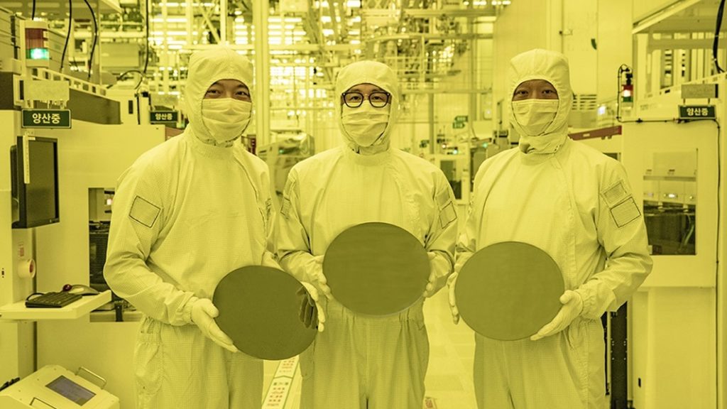
Samsung began chip production using its 3 nm process technology with Gate-All-Around (GAA) transistor architecture in June 2022. Dr. Siyoung Choi, President and Head of Foundry Business at Samsung Electronics, noted that It is the world’s first 3 nm process with Multi-Bridge-Channel FET (MBCFET), Samsung’s GAA technology with improved power efficiency and enhanced performance.