Zen 5 Architecture


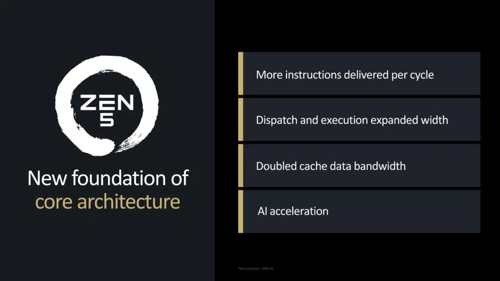
The new content today, coming straight from AMD pre-launch is more information in regards to the architecture changes made with the Zen 5 architecture this generation. Primary goals include more instructions delivered per cycle, dispatch and execution expanded width, doubled cache data bandwidth, and AI acceleration.
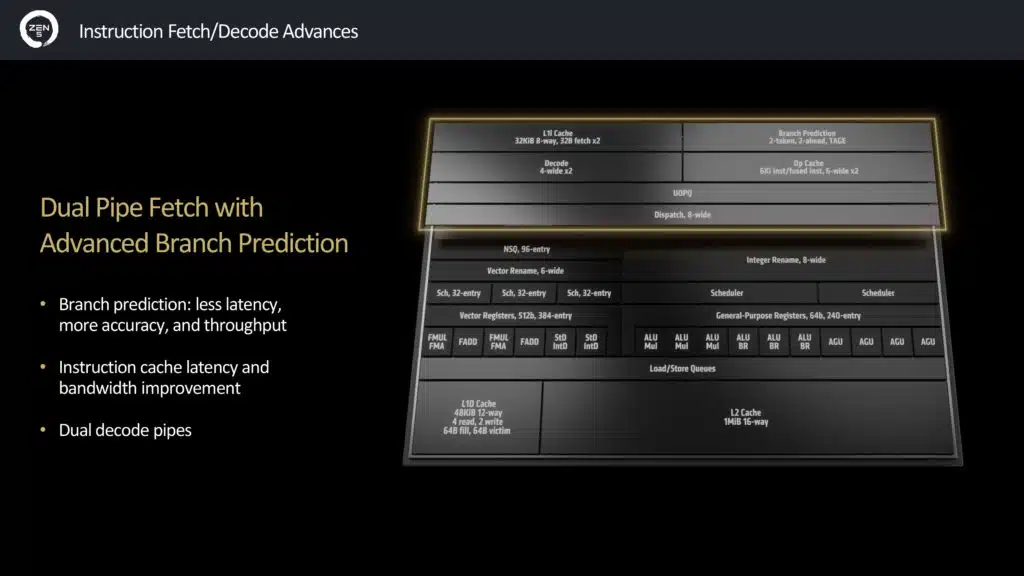
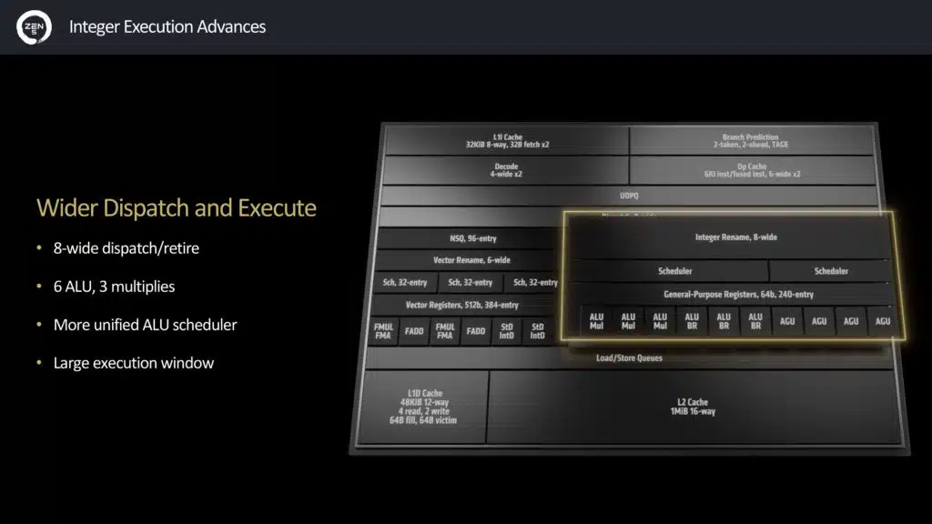
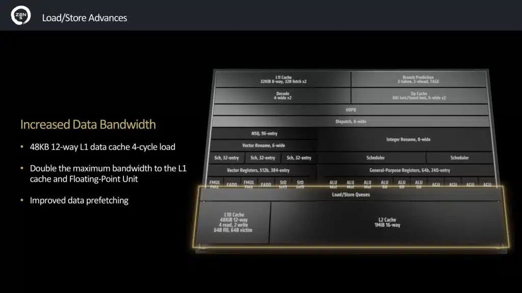
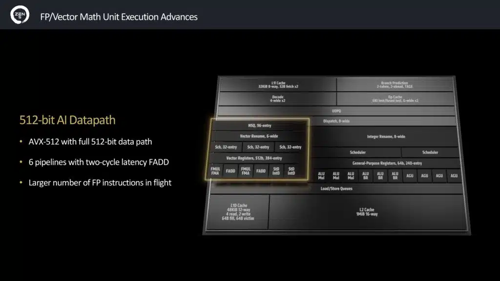
Above you will find the CPU pipeline itself, and the separate sections with benefits shown. Dual Pipe Fetch with Advanced Branch Prediction, less latency, more accuracy and throughput. Instruction cache latency and bandwidth improvement and dual decode pipes. Wider Dispatch and Execute with 8-wide dispatch/retire, 6 ALU, 3 multiplies a more unified ALU scheduler, and a larger execution window. Increased Data Bandwidth with 48KB 12-way L1 data cache, 4-cycle load. Double the maximum bandwidth to the L1 cache and floating-point unit and improve data prefetching. 512-bit AI Datapath with AVX-512 with full 512-bit data path, 6 pipelines with two-cycle latency FADD, a larger number of FP instructions in flight.
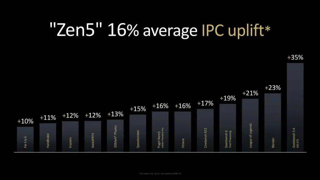
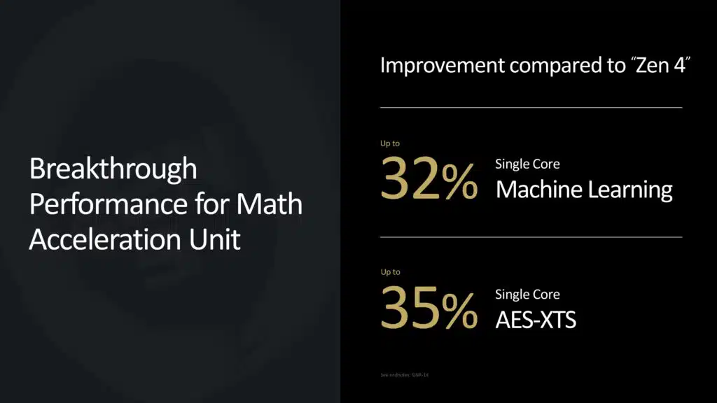
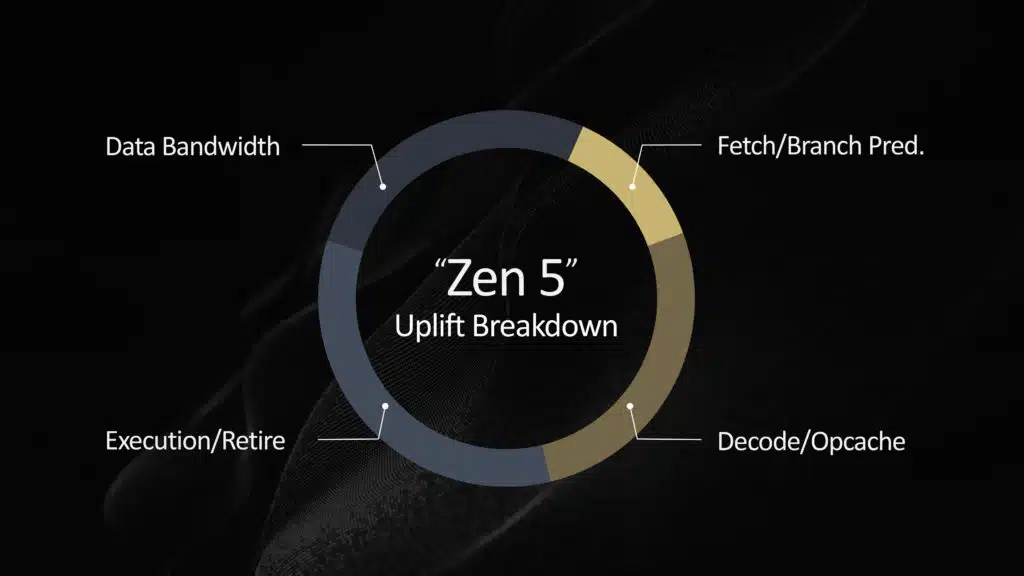
All of this means an average of 16% IPC uplift, a geomean of the slide shown above, it is going to be app dependent, and keep in mind that IPC is not performance. AMD is claiming a 32% improvement in single-core machine learning and a 35% single-core AES-XTS performance. All combined, the culmination of IPC uplift is from data bandwidth, fetch/branch prediction, execution/retire and decode/opcache.
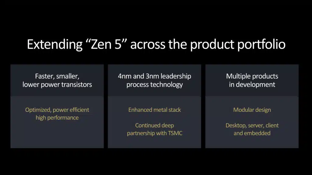
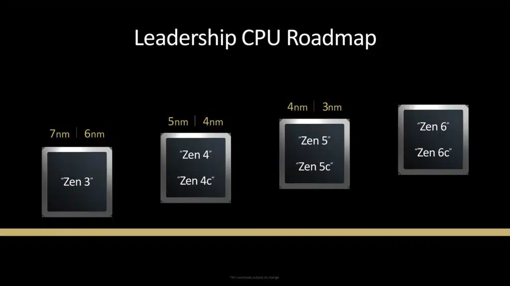
There is also a node improvement and continued leadership in node process technology and modular designs.
RDNA 3.5 Architecture
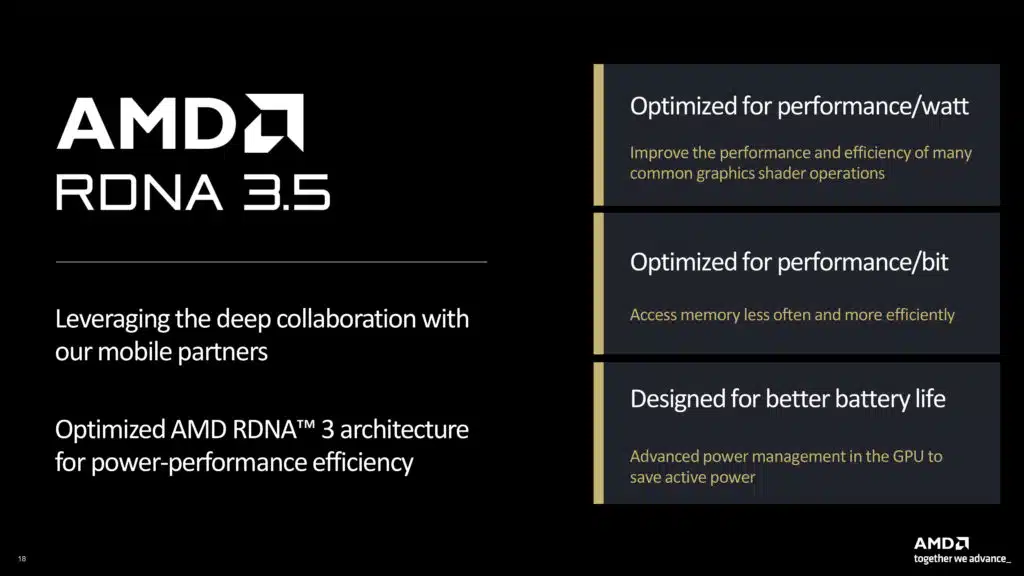
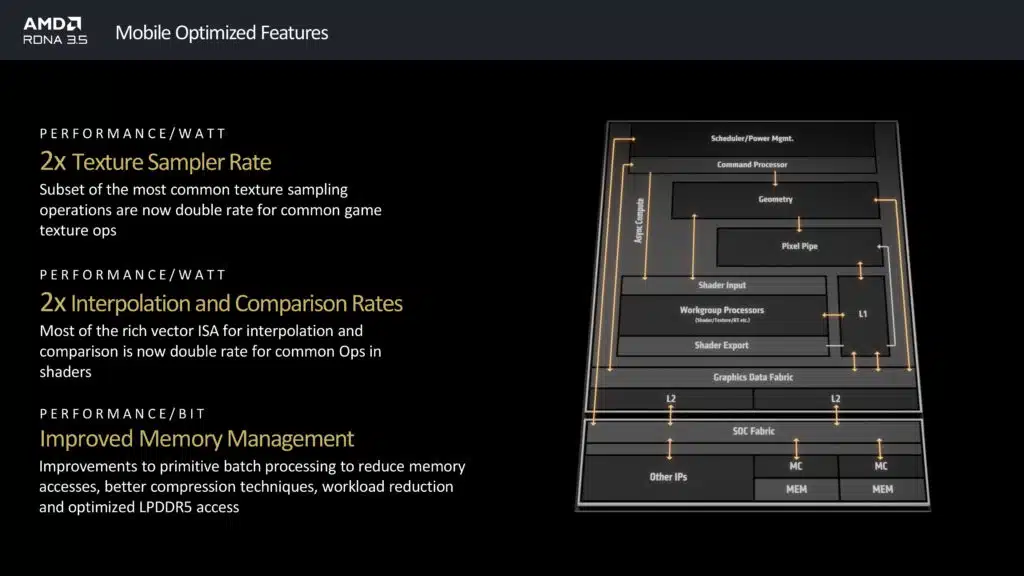
AMD is also finally showing off some information in regards to the changes in the RDNA 3.5 architecture found within the Ryzen AI 300 series mobile processors. RDNA 3.5’s design goals are to optimize for performance per watts, performance per bit, and designed for battery life, which all make sense for a mobile platform.
The changes start with a 2x Texture Sampler rate by now performing a double rate for texture ops on the most common texture sampling operations in the cores. This continues with performing now double-rate ops in shaders for interpolation and comparison in the cores. Finally, improved memory management with batch processing to reduce memory access, better compression, and workload reduction optimized for LPDDR5. Ultimately, with reduced memory access power can be saved on mobile platforms.
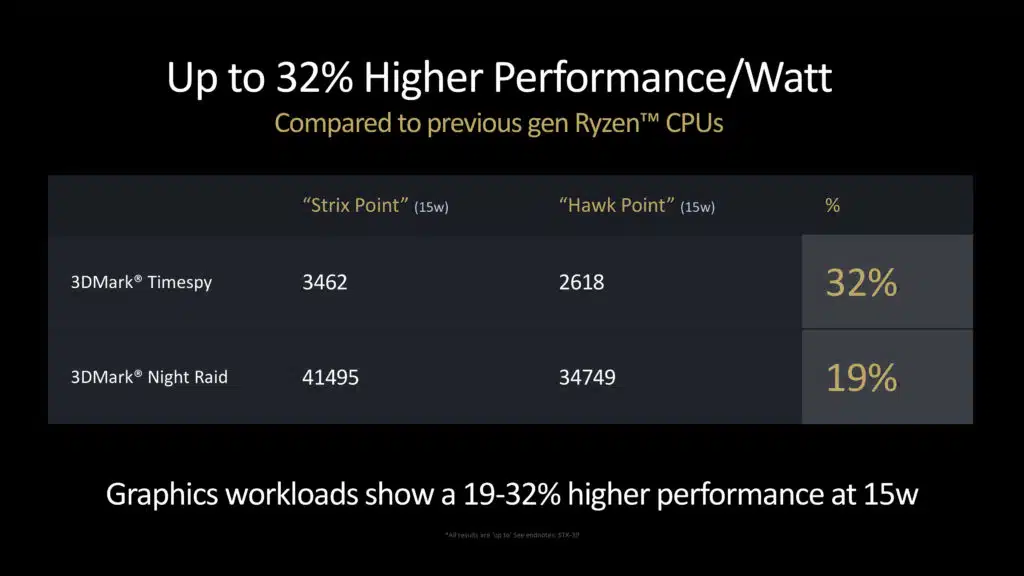
AMD is claiming that in 3DMark Timespy Strix Point should be 32% faster, and 19% faster in 3DMark Night Raid. Therefore, performance in this synthetic benchmark is between 19%-32% faster than Hawk Point at the same Wattage.