Getting CDNA 4 AI compute into a standard rack-mount server has been harder than it should be — until today. AMD has officially launched the Instinct MI350P, a PCIe add-in card based on its CDNA 4 architecture, and it’s the first Instinct GPU in this form factor in roughly four years. The pitch is simple: slot it into an existing air-cooled server, skip the Open Accelerator Module infrastructure, and start running inference workloads. AMD is clearly targeting enterprise customers who want MI350-class performance without having to rebuild their data center around it.
The MI350P is built on CDNA 4, fabricated on TSMC’s 3nm and 6nm FinFET nodes. The card carries 128 Compute Units, 8,192 Stream Processors, and 512 Matrix Cores, with a peak engine clock of 2.2 GHz. Those specs are effectively half of what AMD’s OAM-based MI350X/MI355X offer — a deliberate design choice to keep the card within PCIe power limits. Memory is 144GB of HBM3E across a 4096-bit interface at 4 TB/s peak bandwidth, plus 128MB of last-level cache with full-chip ECC. Peak performance lands at 4.6 PFLOPS at MXFP4 and 2.3 PFLOPS at MXFP8, while FP64 throughput sits at 36 TFLOPS.
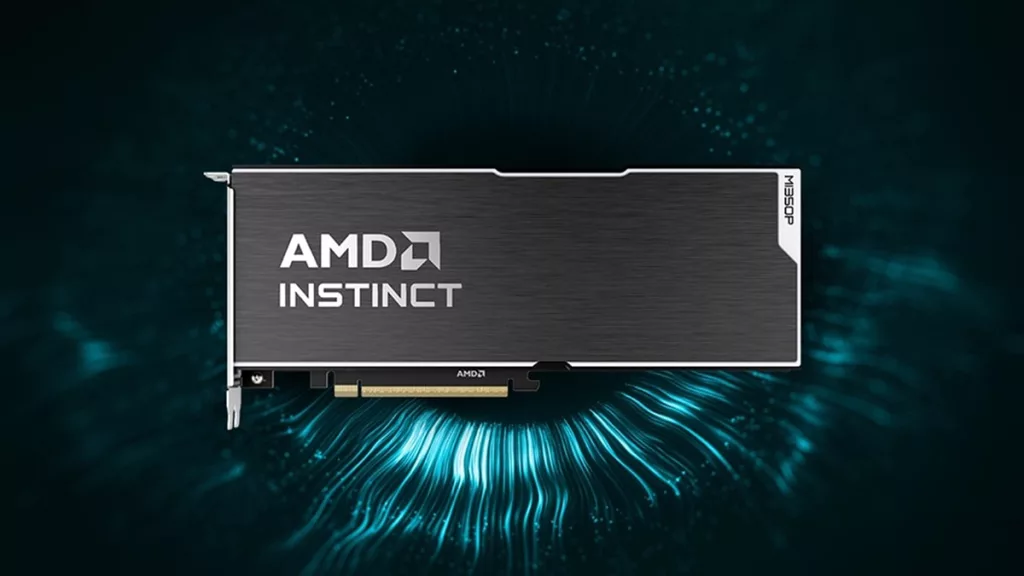
AMD has rated the MI350P at 600W TBP, which happens to be the ceiling defined by the PCIe CEM specification. For servers that can’t support the full thermal load, a 450W mode is available with some performance shaved off. The card uses a 12V-2×6 power connector, making it AMD’s first Instinct product with that plug. It also uses a standard 10.5-inch dual-slot FHHL form factor, so it drops into any server that can fit eight FHHL accelerators — including systems like the Dell PowerEdge XE7740 and HPE ProLiant DL380a Gen12, both designed specifically for dense 600W-class PCIe card arrays. One trade-off worth noting: unlike the MI350X, the MI350P does not expose AMD’s Infinity Fabric scale-up links. All collective communication goes through the PCIe 5.0 x16 host interface, which delivers 128 GB/s.
The competitive context here is NVIDIA’s H200 NVL, which offers 141GB of HBM3E and runs the Hopper H200 die. AMD is claiming the MI350P is roughly 40% faster in FP16 and FP8 theoretical compute compared to the H200 NVL, though AMD-supplied theoretical comparisons always deserve the standard disclaimer about real-world delivered performance. AMD is also emphasizing ROCm open-sauce software support and no-cost development stack access as differentiators from NVIDIA’s more proprietary ecosystem.
Eight MI350P cards in a single air-cooled 2U chassis puts 1,152GB of HBM3E and 32 TB/s of aggregate memory bandwidth in one box. For inference on large open-weight models, that’s enough headroom to host a trillion-parameter model at MXFP4 in a single chassis — which is genuinely interesting for enterprises that want to run those workloads on-premises without NVLink or OAM fabric. Whether they’ll pay for it when H200 NVL hardware is still widely available in the $30-40K range is the real question. The MI350P is available now through AMD’s partner network. AMD has not publicly stated pricing.