AMD is almost certain to release Ryzen chips produced on TSMC’s future 3 nm process, but while those are still a long way off (the company’s 5 nm “Zen 4” processors are still a year or two away), we are beginning to learn what they could be packing.
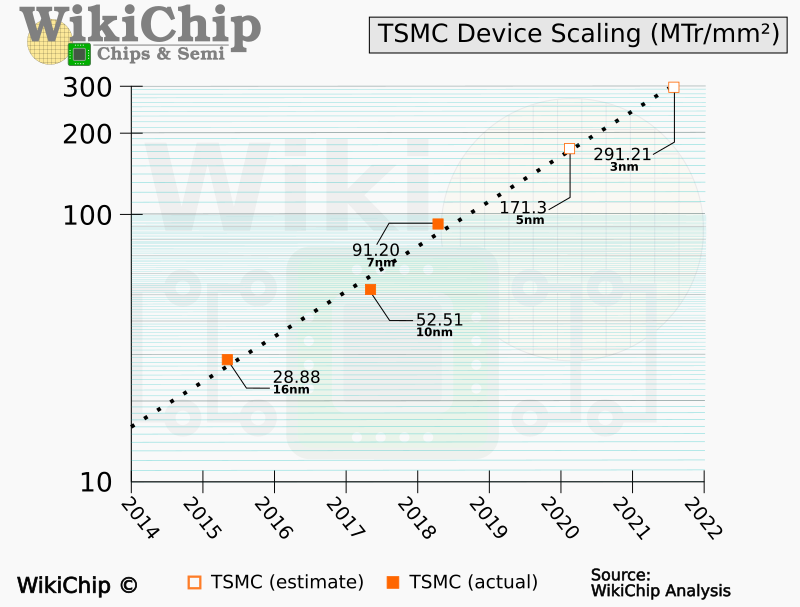
According to a WikiChip report, TSMC’s N3 (3 nm) node will feature a 1.7x improvement over N5, which is equal to a density of almost 300 million transistors per square millimeter. TechPowerUp puts that into perspective by equating that to shrinking a Pentium 4 processor die to the size of a pinhead.
During his latest earnings call, TSMC CEO Dr. C. C. Wei confirmed that the N3 node is on track, with risk production scheduled for 2021. “TSMC is targeting volume production in the second half of 2022,” WikiChip wrote. “The company says that after evaluating all the possible device technology options, it had decided to continue with FinFET for N3 due to its maturity, performance, and cost advantages.”
As for N5 (which AMD will leverage for its 4th Gen, Zen 4-based “Genoa” processors), that node will deliver “around 1.8x improvement in density along with 15% higher speed at iso-power or, alternatively, 30% lower power at the same speed,” reported WikiChip. “TSMC estimates that N5 will contribute about 10% of wafer revenue in 2020. TSMC is observing a higher number of tape-outs compared to N7 at the same period of time during their ramp.”