AMD Lead Engineer Sam Naffziger recently provided a presentation covering the AMD Radeon 7000 graphics card announcements. Afterward, Steve Burke (GN) was able to get a little extra time after the presentation to go over highlights while also covering some questions. The PC community has seen a number of changes since multiple GPU configurations such as AMD Crossfire or NVIDIA SLI effectively came to an end. Each company is moving beyond them with new approaches. While NVIDIA has invested itself into RT Cores and Tensor Cores combined with DLSS, AMD has focused on chiplets, compute units and FSR.
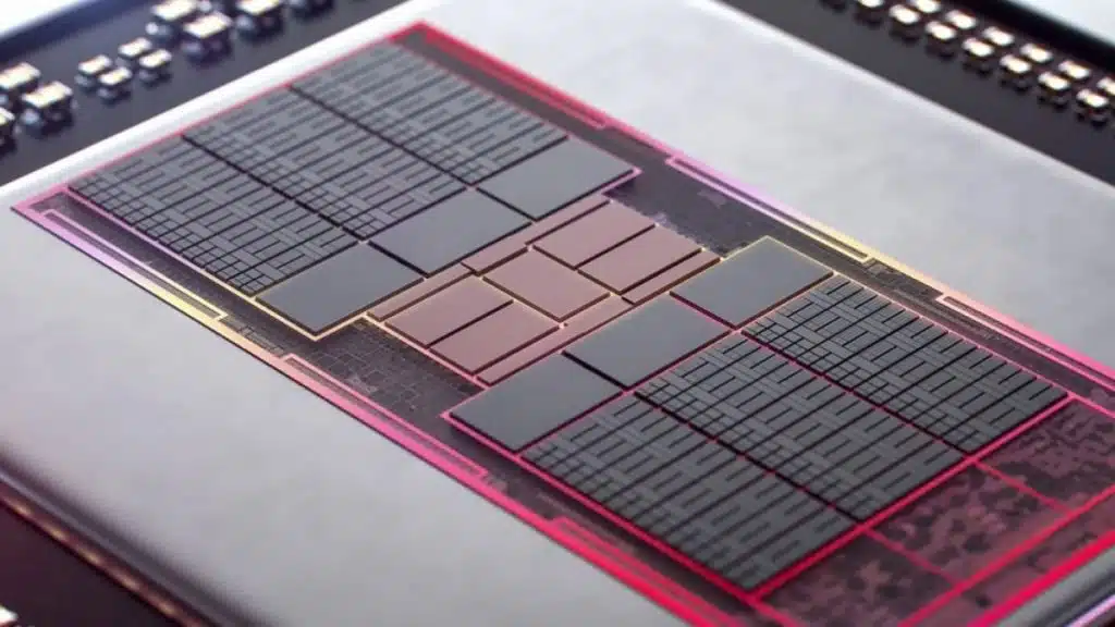
AMD Lead Engineer Sam Naffziger previously worked on introducing chiplet designs with the Ryzen Zen and Epyc line of processors in 2016 but explains in this follow-up presentation that incorporating them into AMD’s RDNA3 GPUs doesn’t follow the exact same approach but does still yield cost-saving rewards and performance improvements. It was towards the end of 2017 that he moved on to AMD’s graphics card division to begin developing the RDNA3 chiplet architecture.
Sam begins by identifying three factors of scale improvement for SoCs, CPUs, and GPUs: analog I/O, memory cache, and logic. While logic has managed to continue to make gains with shrinking nodes analog I/O and memory cache have nearly flatlined in terms of performance gains since moving from 7nm. In an ironic twist, potential manufacturing cost savings are lost since even though the die has shrunk the other factors remain mostly the same and those costs continue to rise. However, one advantage that is maintained with the shrinking node is logic power consumption.
Enter GPU chiplets
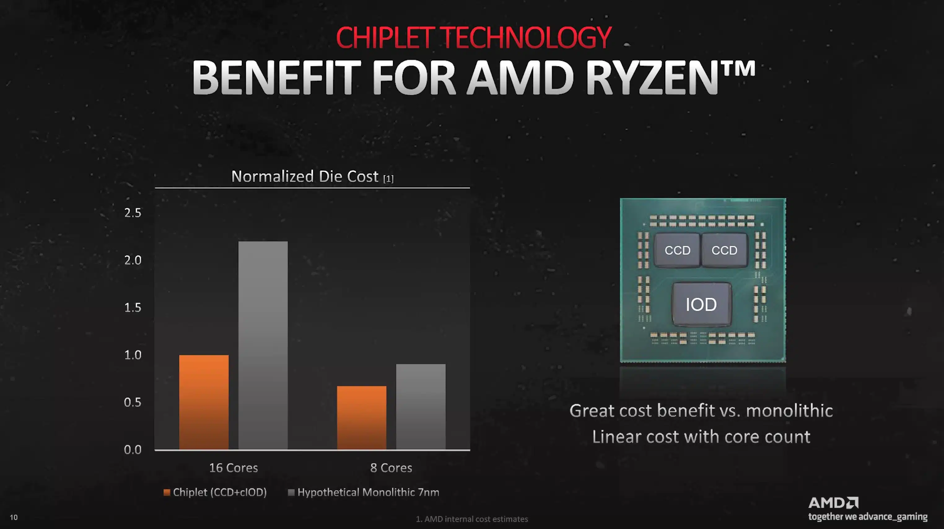
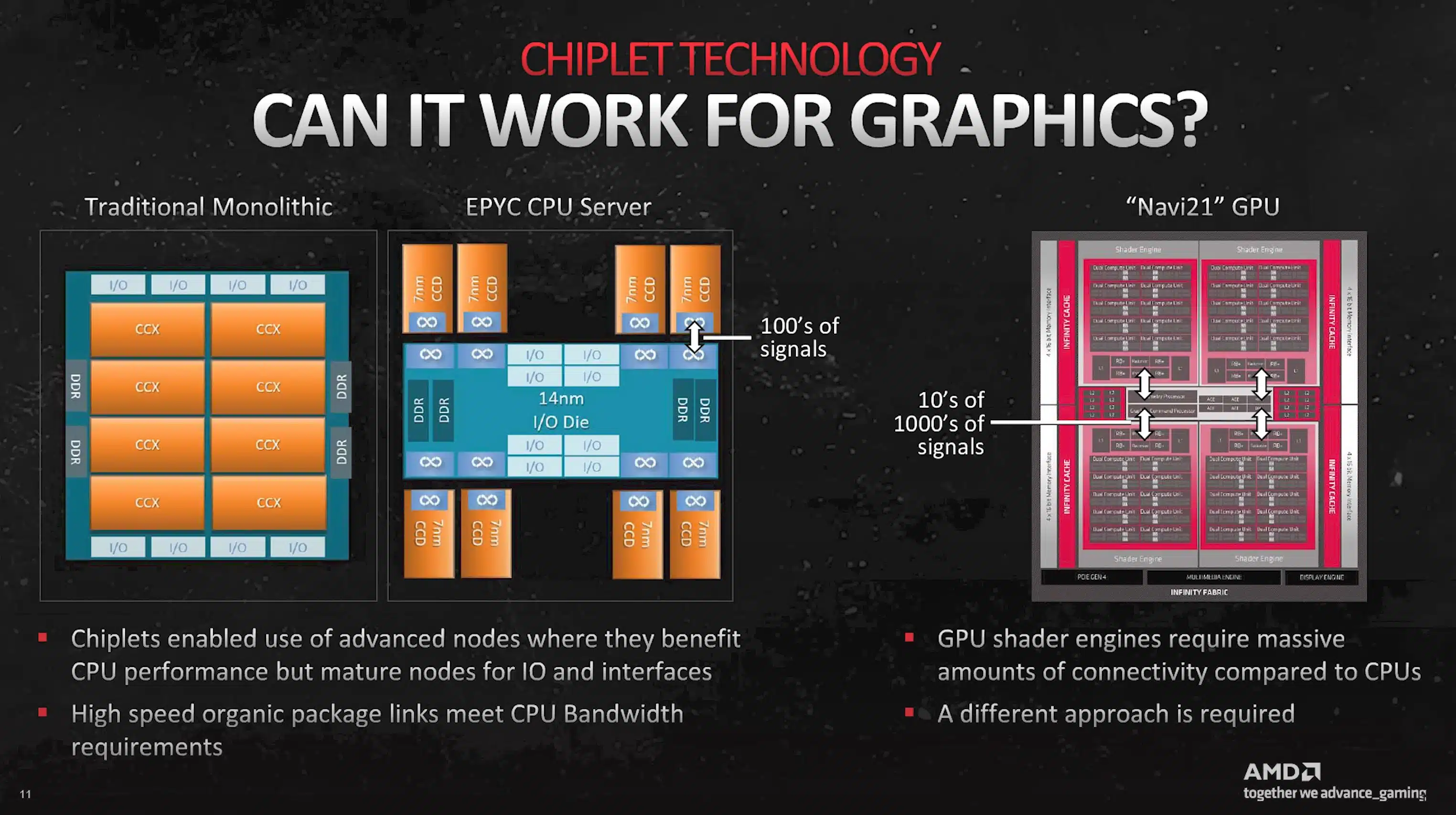
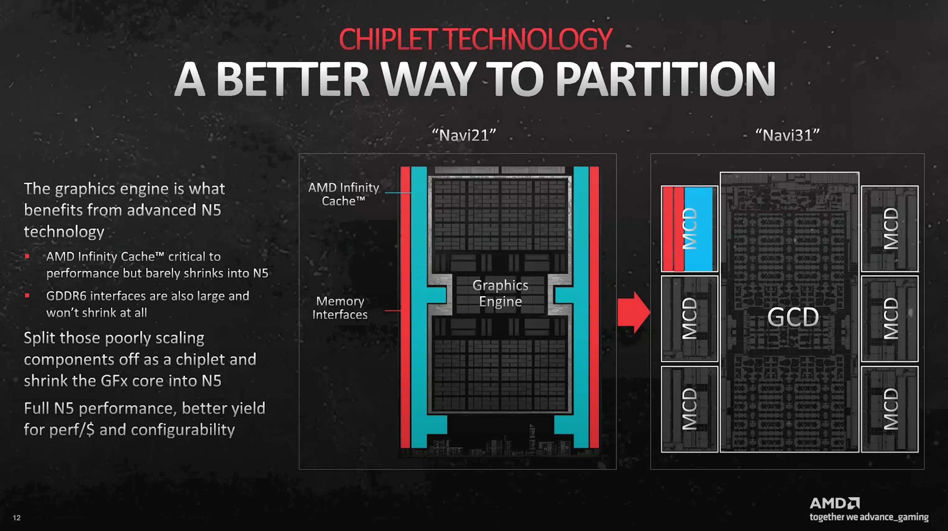
Mr. Naffziger explains that by using chiplet designs for CPUs and GPUs manufacturing costs are significantly reduced but they also allow an easier path for product refreshes, or new architecures, along with improved yields in regards to wafer defects. In adapting chiplets to GPUs different nodes can be adapted for DDR memory, PCI express, bandwidth, and other GPU-specific tasks, versus a complete die redesign thus reducing the resources needed to develop a new GPU or adapt it to newer technology. AMD’s Infinity Fabric has been adapted for RDNA3 to provide an industry-leading 5.3 TB/s of peak bandwidth, almost 10x more than previously seen with Ryzen and Epyc. Sam finishes by showing how using a chiplet approach also allowed further die shrinkage by partitioning DDR6 interfaces to them.