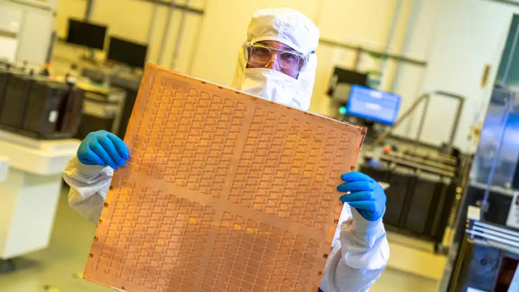
Intel has announced that it plans to deliver its first complete glass substrate solutions later this decade. Designed to deliver even more powerful compute and advance Moore’s Law with the continued scaling of transistors, Intel says that glass provides numerous benefits over existing organic solutions, such as improved rigidity, higher temperature tolerance, and far less pattern distortion, enabling more chips to fit onto a single package. As much as 50% more die content can fit on the same package size versus organic substrates, according to a 60-second primer that Intel shared.
“After a decade of research, Intel has achieved industry-leading glass substrates for advanced packaging. We look forward to delivering these cutting-edge technologies that will benefit our key players and foundry customers for decades to come,” said Babak Sabi, Intel senior vice president and general manager of Assembly and Test Development.
Glass substrates will initially be introduced into the market where they can be leveraged the most: applications and workloads requiring larger form factor packages (i.e., data centers, AI, graphics) and higher speed capabilities.
Glass substrates can tolerate higher temperatures, offer 50% less pattern distortion, and have ultra-low flatness for improved depth of focus for lithography, and have the dimensional stability needed for extremely tight layer-to-layer interconnect overlay. As a result of these distinctive properties, a 10x increase in interconnect density is possible on glass substrates. Further, improved mechanical properties of glass enable ultra-large form-factor packages with very high assembly yields.
Glass substrates’ tolerance to higher temperatures also offers chip architects flexibility on how to set the design rules for power delivery and signal routing because it gives them the ability to seamlessly integrate optical interconnects, as well as embed inductors and capacitors into the glass at higher temperature processing. This allows for better power delivery solutions while achieving high-speed signaling that is needed at much lower power. These many benefits bring the industry closer to being able to scale 1 trillion transistors on a package by 2030.