Block diagrams rumored to be for AMD’s upcoming UDNA GPUs indicate some very interesting changes ahead, including a new flagship design. Perhaps one of the funnest moments during a generational release happens towards the end of the cycle when rumors about the next begin to ramp up. For those on the hunt for what’s next, it’s akin to looking forward to a potential long-desired birthday or holiday gift. Well, AMD fans, those holding onto hopes for a new top-tier consumer GPU, which AMD intentionally skipped with the Radeon 9000 series, may have reason to celebrate with UDNA (also known as RDNA 5).
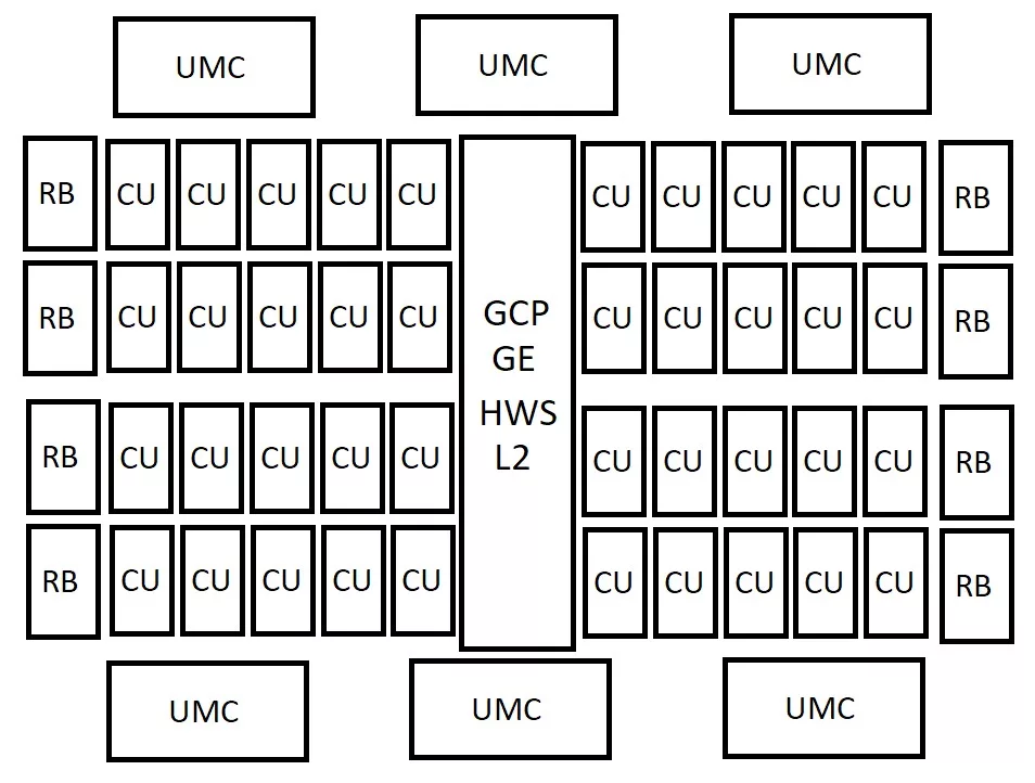
Well-known hardware information leaker Kepler has posted block diagrams for four different GPU designs on the Anandtech Forums (via Wccftech). At the top of the potential GPU stack is a product seemingly intended to compete with NVIDIA’s GB202 (RTX 5090) die. It has 96 compute units split into 8 shader arrays, with each array containing 16 shader engines and each engine with 6 CUs. This GPU also has 16 unified memory controllers, each 32-bit, leading to a 512-bit bus, but could be 384-bit if 16-bit memory is used. It’s suggested that this silicon could feature up to 128 MB Infinity Cache as well, but this may change if AMD alters the design currently used in RDNA 4. Max VRAM size could be up to 32 GB.
Next up are what could be considered a mid-range layout and then something that could be configured as needed to offer a budget range or potential mobile GPU offerings. As far as mobile dGPU offerings, AMD has primarily relied on its APUs featuring iGPU graphics, so it would be interesting to see if it is considering a mobile discrete option given the success of its APUs on many fronts. There is a possibility the low-end design could be integrated into an APU package.
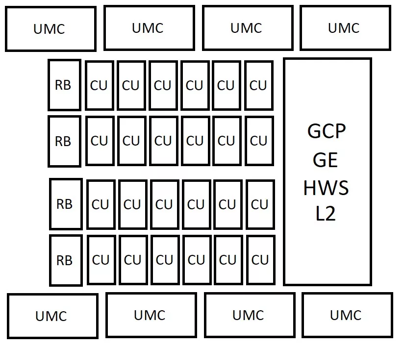
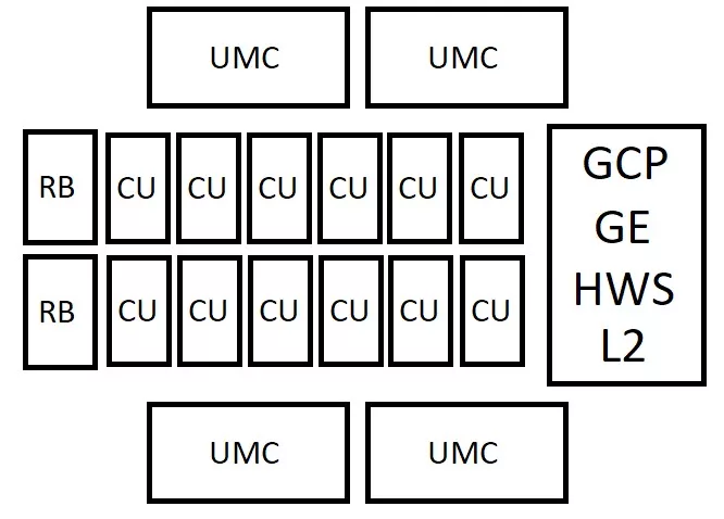
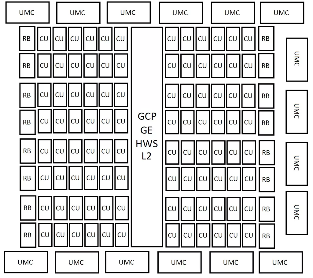
Meanwhile, AMD has held its own in trading blows with NVIDIA at the mid-range tier level and still competes well at the budget level with Team Green and Intel. According to the design layouts, the mid-range GPU would feature 40 CUs split among 8 shader engines, each with 5 CUs arranged into 4 arrays. Memory configuration for this die includes 6 unified memory controllers on a 192-bit bus (12 GB VRAM) and possibly 48 MB of Infinity Cache. If 32-bit memory is used, VRAM could be 24 GB. Next down the line is what appears to be a budget-oriented die with 24 CUs and 8 memory controllers on what could be either a 256-bit bus (if using 32-bit memory/16 GB) or a 128-bit bus (if using 16-bit memory/8 GB). Lastly is a design feature just 12 CUs spread across 2 shader arrays. Memory for this die could be either 128-bit or 64-bit. Infinity Cache for both is said to be 32 MB.