Has the AMD Radeon VII matured?
Introduction
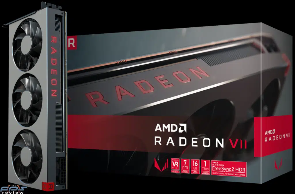
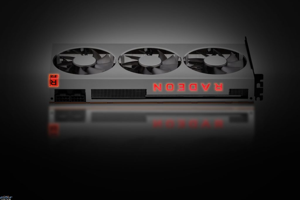
AMD launched its Radeon VII video card on February 7th, 2019 with an MSRP of $699.99. This enters AMD’s attempt at the high-end gaming video market, but also taps into the content creators’ market as well. It’s a bit of a dual-wielding video card, built for gaming and professional use. This does supersede the AMD Radeon RX Vega series in performance. Those video cards were not high-end.
It has been nearly four months since its official launch. Since that time there have been several new driver versions released with optimizations along the way. There has also been a new BIOS since its release. As we know, GPU performance, especially on updated architectures take time to mature. Generally over time performance goes up and bugs get squashed.
The question is, since its launch has performance changed or improved over time up to this summer? What is the performance like right now in modern games with the AMD Radeon VII video card? New games have been released since the video card was launched, and we need to see how this video card performs in those games. We are going to answer these very questions in this gaming oriented review today.
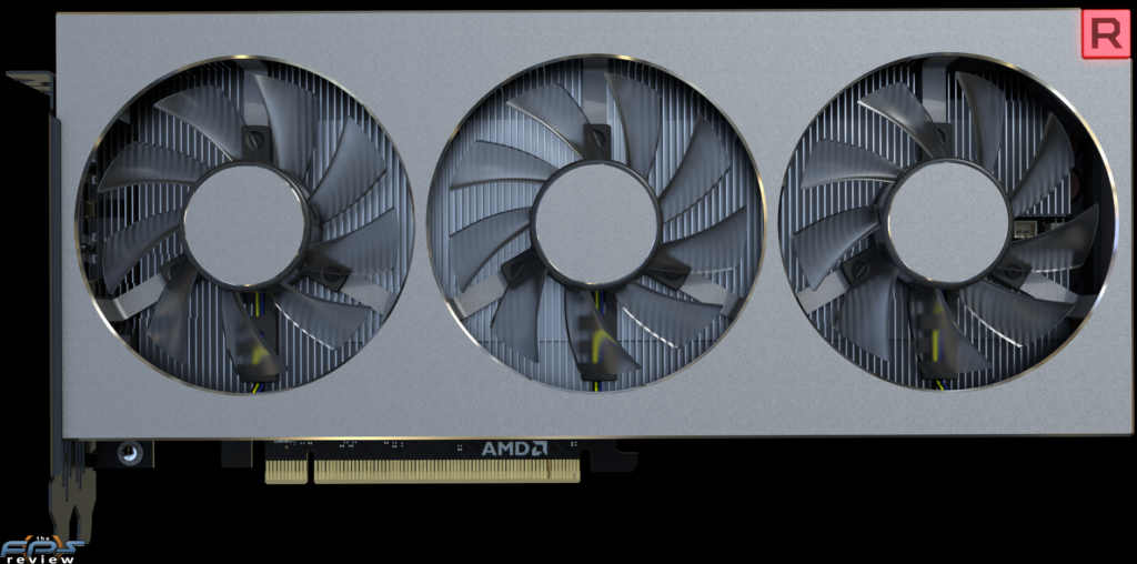
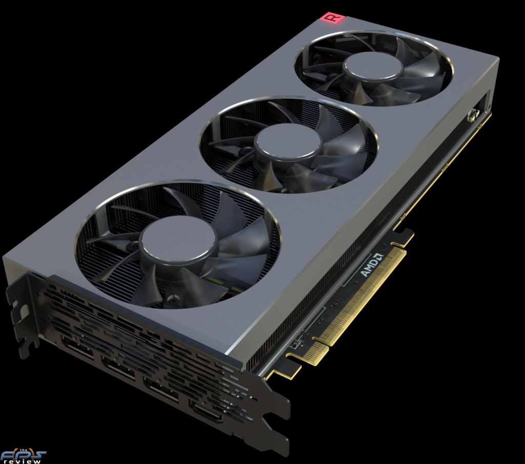
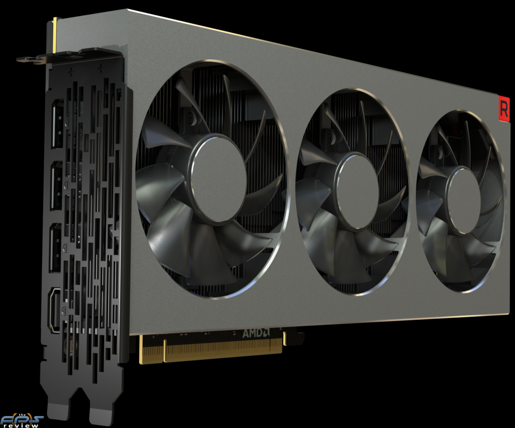
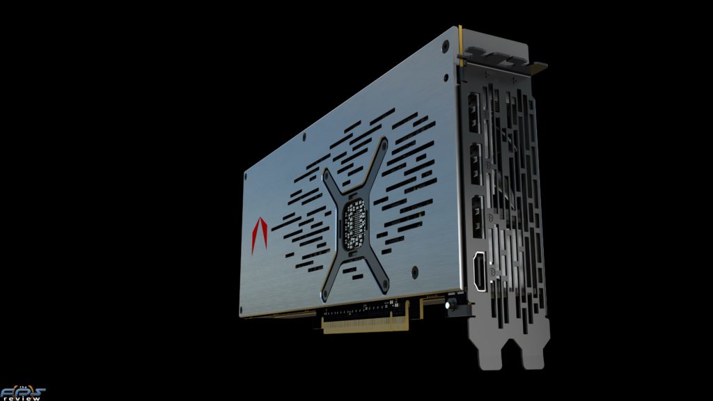
AMD Radeon VII
What makes the AMD Radeon VII truly unique are a set of features that are still very new to the industry. The AMD Radeon VII is in some ways forward looking in technology. AMD utilizes TSMC’s 7nm node manufacturing process for the GPU, at this specific time this is still the only consumer gamer-oriented GPU that is made in this way. 7nm is where everyone is going, on CPU and other GPUs in the future.
AMD’s transition to the 7nm process puts it ahead on production maturity with the new node. The benefits are lower power, and faster performance. This year is going to be the year of 7nm finally, the Radeon VII paved the way and this summer we think you’ll be seeing a lot more 7nm hardware.
The other key forward looking architectural improvement is the use of 4096-bit HBM2 memory stacked running at 2GHz on the AMD Radeon VII. Utilizing this new memory is another step into the future. All of this allows a whopping 1TB/sec of memory bandwidth. This is by far the most memory bandwidth ever released on a consumer gaming-oriented video card.
In addition, AMD has equipped the AMD Radeon VII with 16GB of this HBM2 memory! That is once again the highest capacity VRAM ever used in a consumer gaming-oriented video card. Technically this video card has bandwidth and capacity to push high resolution 4K and higher gaming, the raw data bandwidth and capacity needed is in place. You should never have stuttering related to running out of VRAM capacity. The only thing holding the video card back is the architecture itself.
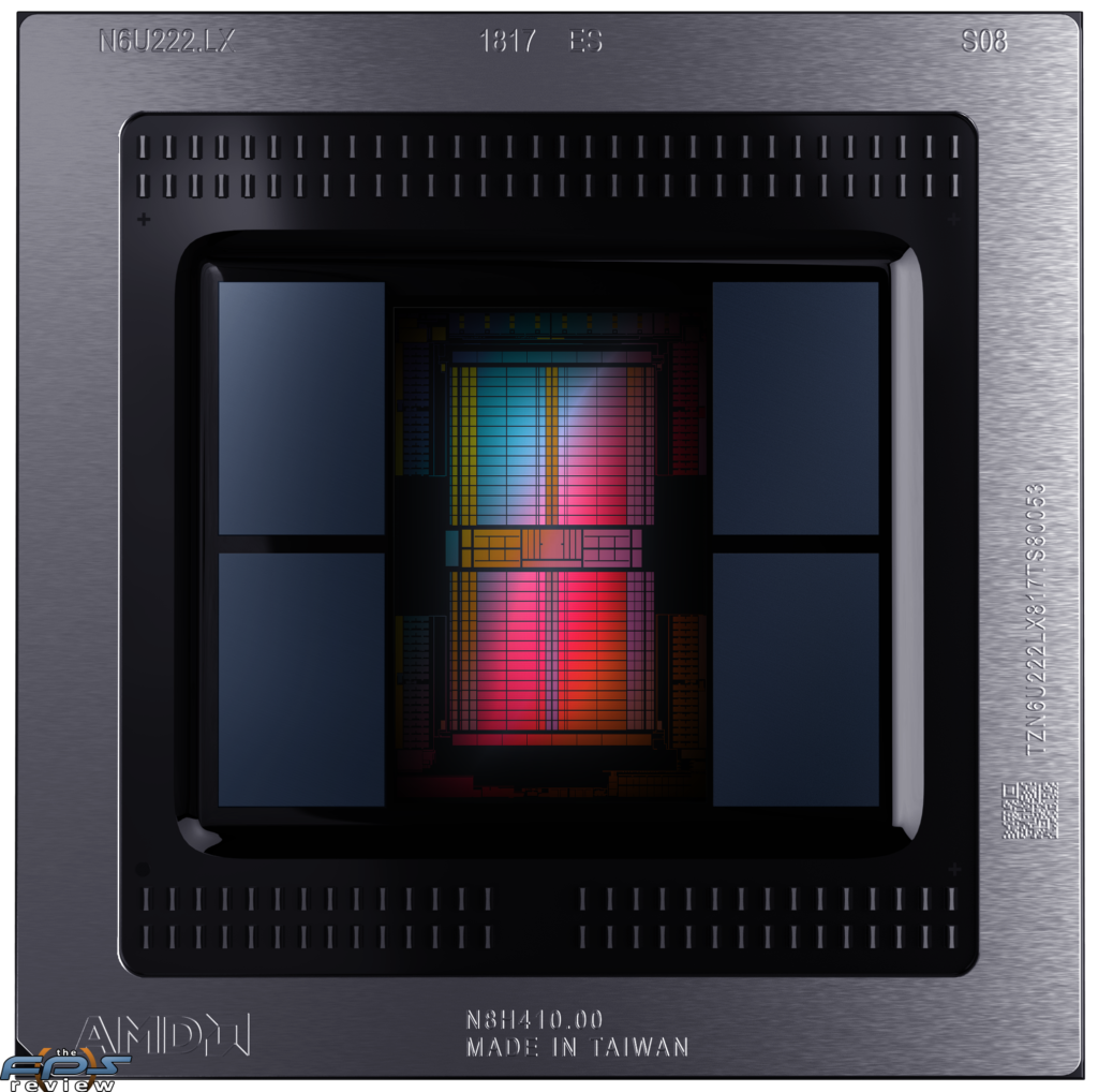
At its core, the AMD Radeon VII is ultimately an evolution of the aging GCN architecture. It uses a refreshed AMD Radeon Vega GCN Vega 20 architecture. This is an aging architecture that is getting very long in the tooth when it comes to pixel pushing power. It is also not the most efficient architecture, requiring a lot of power to run at high frequencies.
The reduction to 7nm manufacturing ability basically means AMD has taken the power savings from that jump and applied it to much higher operating clock frequencies. This, combined with the memory bandwidth is what gives the Radeon VII its performance boost over the AMD Radeon RX Vega 64.
Speaking of which, the AMD Radeon VII has 3,840 Stream Processors versus the Radeon RX Vega 64’s 4,096. The Radeon VII has 60 active CUs, while Vega 64 has 64. It’s a shame really, we would have liked to have seen a fully spec Radeon VII at the new clock speeds, the extra CUs would boost performance well above a GeForce RTX 2080 if it had them. The Radeon VII has 240 Texture Units and 64 ROPs. The Base Clock runs at 1400MHz and the Boost Clock runs at 1750MHz on Radeon VII. This is compared to Vega 64 running at 1546MHz Boost Clock.
As mentioned, the Radeon VII has 16GB of 4096-bit HBM2 at 2GHz providing 1TB/sec of memory bandwidth. The Radeon RX Vega 64 has 8GB of 2048-bit HBM2 at 1.89GHz providing 483GB/sec of memory bandwidth. The Radeon VII has a TDP of 300W while the Radeon RX Vega 64 was 295W. The video card requires two 8-pin PCIe power connectors.