Ryzen 3000 Series Architectural Overview
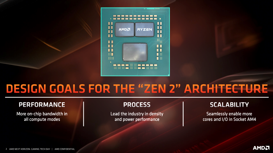
AMD’s Ryzen 3000 series or (Zen 2) is a 7nm die shrink of the Zen microarchitecture. However, it is more than a mere die shrink, but it isn’t an entirely new architecture either. It still resembles the old Zen and Zen+ functionally, but internally the processor has been almost completely re-arranged. AMD states that it was nothing short of miraculous that they were able to maintain socket AM4 compatibility with all the changes. That said, the changes AMD has made have numerous benefits all with the goal of improving performance. Predominantly, performance in single-threaded workloads. Performance improvements in multi-threaded workloads come with some of the improvements to the architecture, but they are also a result of increased core density and clock speeds.

The changes are nothing short of substantial. There are honestly way too many to get into and frankly, you practically need to be an expert and CPU design to fully understand everything that AMD has done to improve Zen 2. For the sake of brevity, I’ll try and keep this as simple as there is allot to cover here. As stated previously, Zen 2 is a process node shrink. When you have a process node shrink, there are many benefits that go with that. Reduced power consumption and or a larger transistor budget are the big ones. AMD has used the process change to increase the CPU’s clocks as well as keep its thermals about the same as what we are used to, if not slightly better. On top of that, there is more space in the package to increase core density and provide more internal resources such as cache.
AMD lists the following as major architectural changes compared to Zen+.
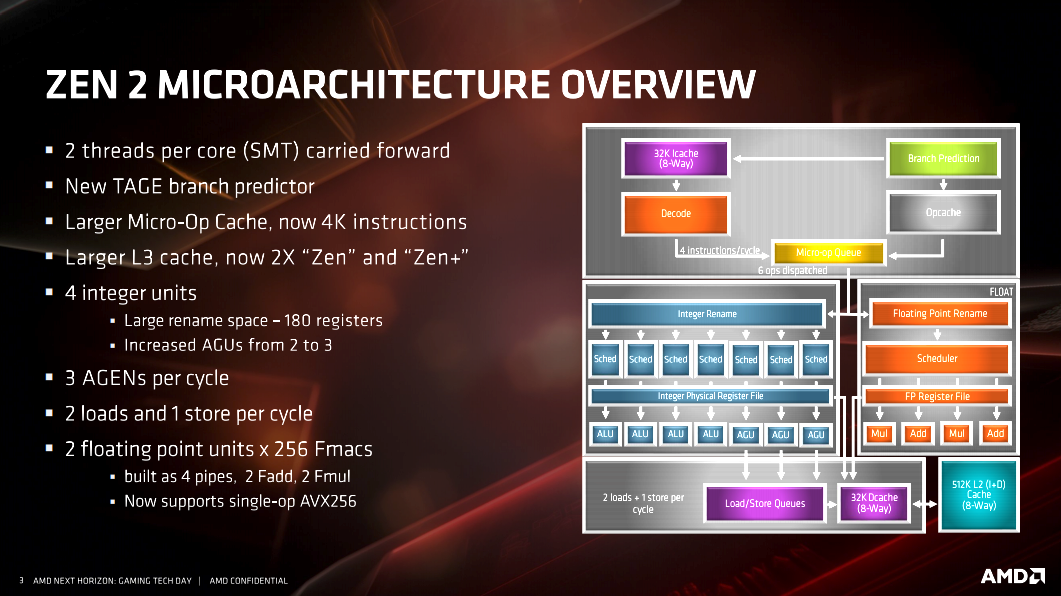
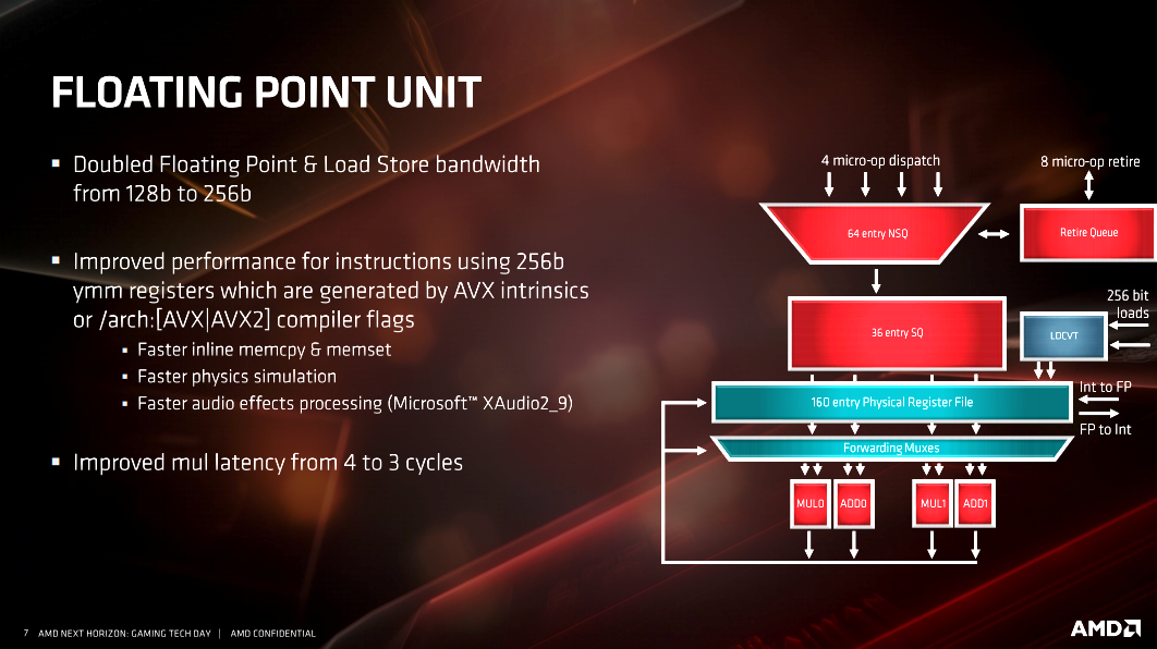
- 256-bit single-op floating point (AVX-256) for notably stronger performance in creative workloads.
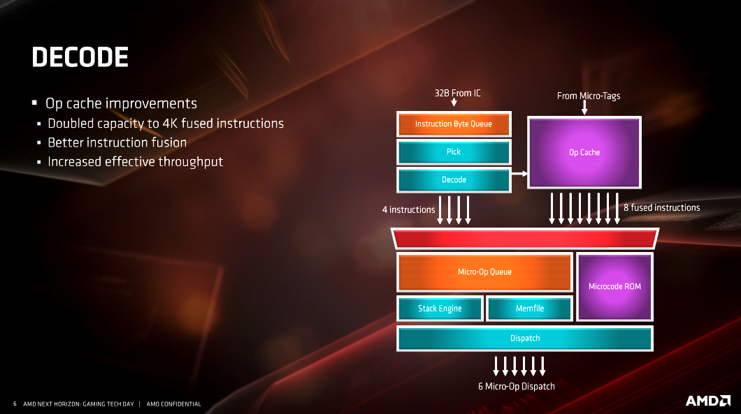
- Doubled Micro-Op cache size (now 4K) to increase throughput by preventing re-decode of operations.
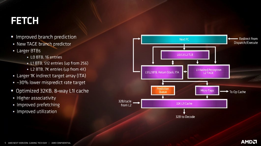
- New TAGE branch predictor, with larger L1 and L2 BTBs, to increase throughput by reducing stalls from mispredicts.
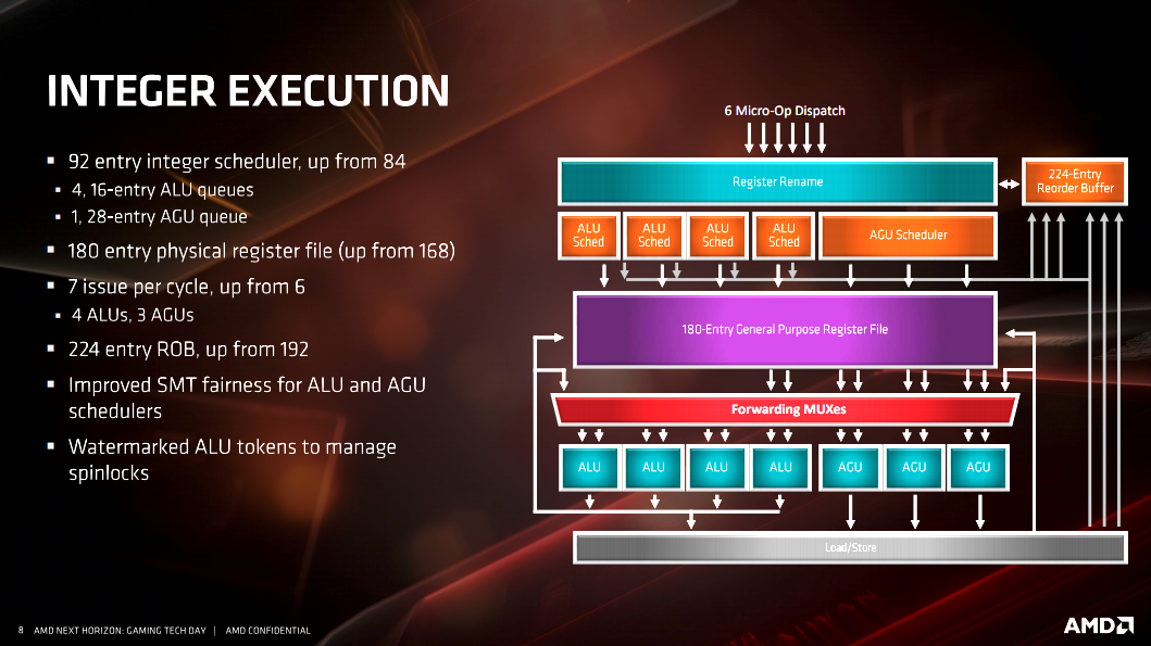
- A third address generation unit (AGU), which keeps the execution engine more reliably fed with data in DRAM.
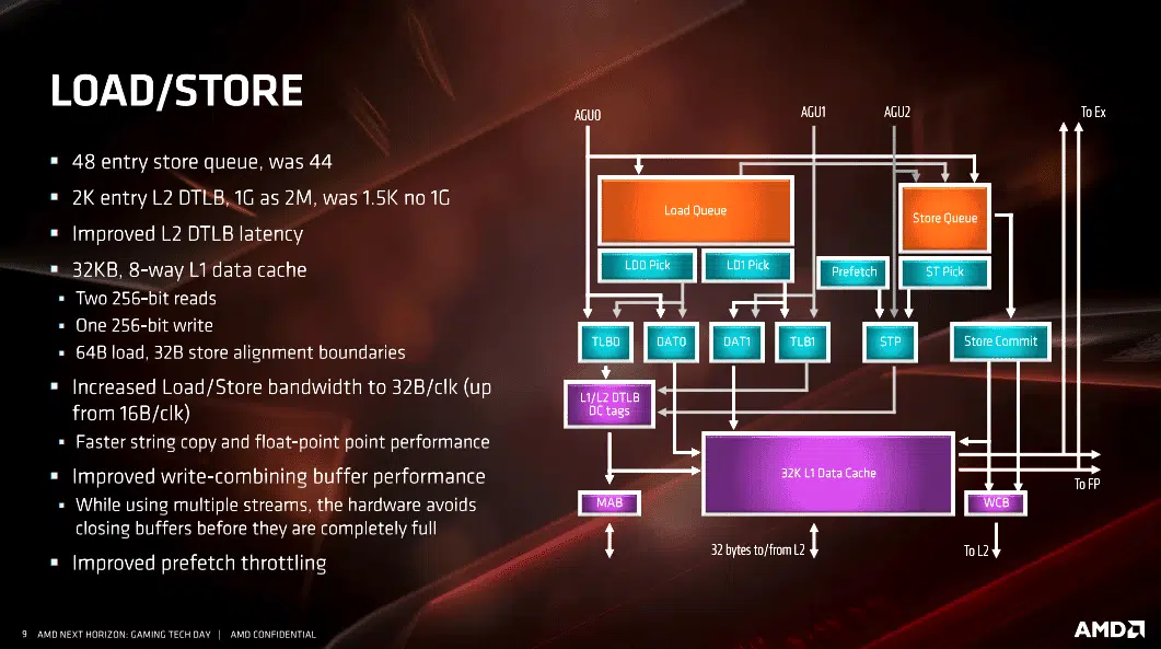
- Improved load/store bandwidth throughout the device, which increases throughput by keeping more data on-chip.
- A doubled L3 cache size to 32MB per CCD, which reduces effective memory latency by up to 33ns—excellent for games.
- Improved fetch and pre-fetch capabilities, arming the execution engines more readily with needed data.
- Improved SMT fairness for ALU and AGU schedulers, reducing thread contention and throughput.
- A larger 180-entry register file, providing the CPU more immediate access to more working data.
- New hardware mitigation against speculative store bypass (Spectre V4), expanding the strong security profile of “Zen(+).”
LEADING TO:
An overall IPC uplift of approximately 15% generationally. Together, these changes enable massive
generational improvements (vs. Ryzen™ 7 2700X) in gaming performance of up to 34% in popular games like CounterStrike: Global Offensive; 30% in League of Legends; and 22% in PUBG, respectively. And when you factor clockspeeds into the mix, the total single-thread performance uplift is up to 21% YoY—an improvement that far outpaces the industry’s yearly gain.
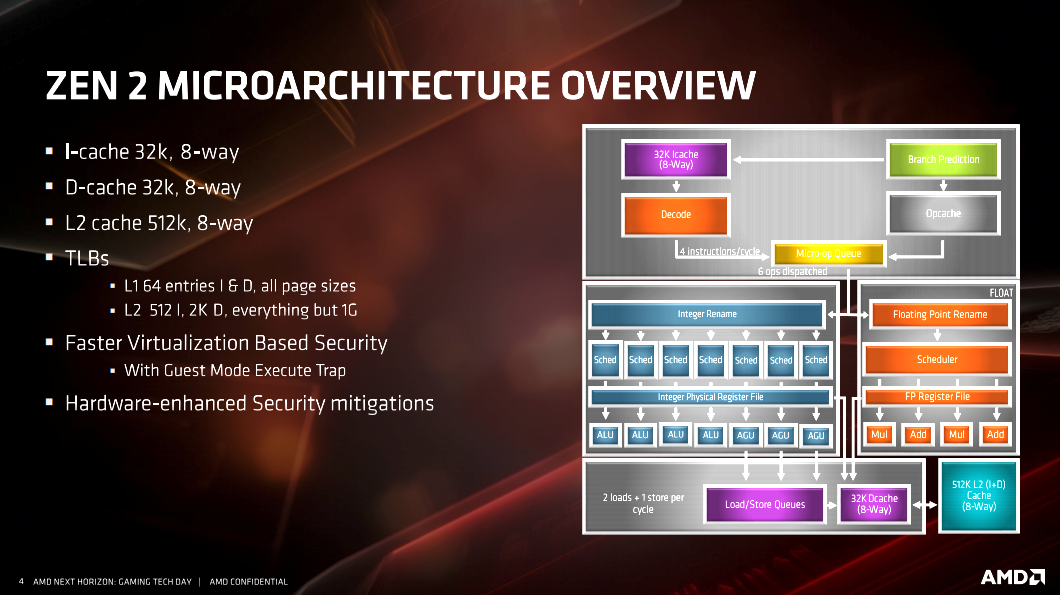
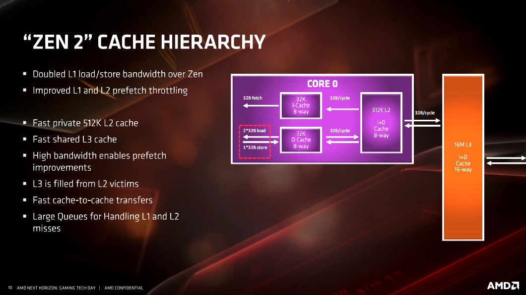
There are a multitude of slides from AMD on the specific architectural changes listed above. I’ve included them here for anyone who wants to dive deeper into the architecture and better understand it. However, as I said, most people reading this aren’t going to fully understand the information AMD is presenting on the slides. Frankly, I don’t understand all of it either. When you get down to it, the improvements to cache, FPU and additional instruction sets accomplish specific goals. The end result of AMD achieving those goals are worth understanding.
Cache improvements, naturally speed up overall performance. Specifically, L3 cache improves performance in games and any cache sensitive application. I’ll talk more about this in detail later on in the article.
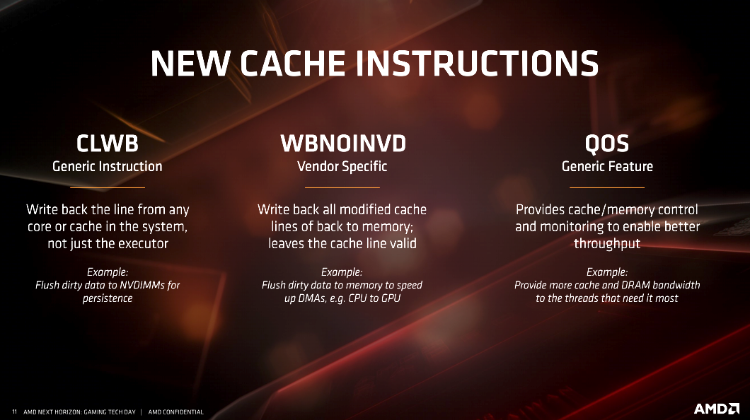
Improvements to the FPU result in better AVX/AVX2 performance. This means faster encoding. The new instruction sets improve security through better mitigation of vulnerabilities like Spectre. The QoS cache instructions have the potential for improved performance in virtualization. The example given in the slide specifically calls out providing more cache and more DRAM bandwidth to the threads that need it the most. A case for this would be where a specific VM is heavily utilized. QoS can prioritize this VM and ensure it gets the required resources.
We already covered the improvements to the memory controller in the X570 platform portion of this article. However, I’ll reiterate that the improved controller supports 128GB of DDR4 RAM. ECC is supported, but it is up to the motherboard manufacturers to enable it on specific models. The relationship between the memory, unified memory controller, and the Infinity Fabric, needs to be understood as they can have a direct impact on performance.
Chiplet Based Design
Physically, the CPU’s look identical to their predecessors outside of the markings on the heat spreader. However, internally, they are considerably different. AMD has switched from a monolithic homogenous die to a “chiplet” design. A chiplet design contains multiple heterogenous dies with different functions. For those who are unaware, a monolithic design means that the CPU is essentially, a one-piece design. A chiplet based design combines multiple chiplets to create a CPU. This allows some flexibility in the design and improves yields, scalability, and allows for greater core density. The chiplet design allows various parts to be produced separately and combined to form a desired configuration.
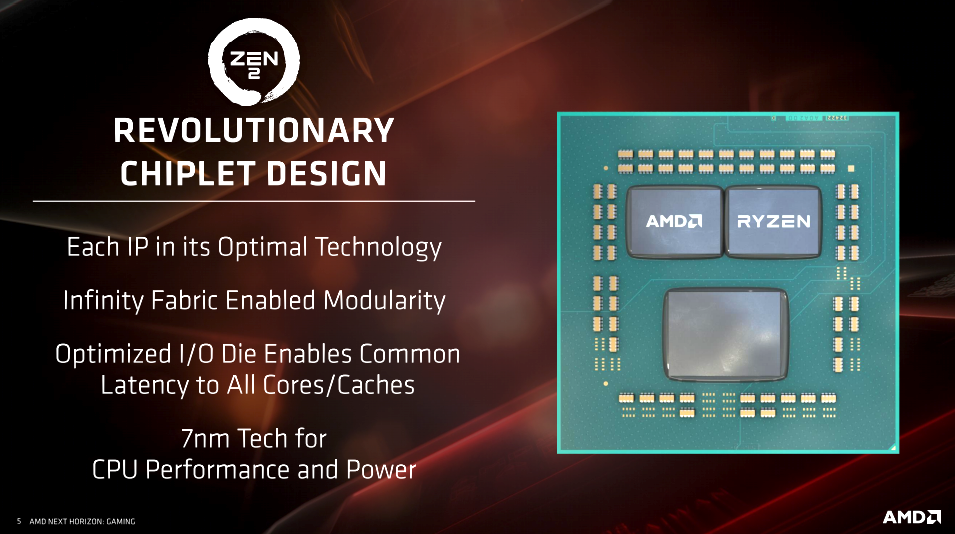
The AMD Ryzen 9 3900X houses three chiplets to form the whole. There are two 7nm ~74mm² CCD’s or “Core Chiplet Dies” within the Ryzen 9 3900X or 3950X. These contain 3.9 billion transistors. Each CCD contains two CCX complexes and dedicated L3 cache for each complex.

The third chiplet is a 12nm I/O die which is ~125mm² in size containing 2.09 billion transistors. The I/O die has been separated as a common interface for each chiplet and its CCX complexes. Every core has the same access latency to the IO die (1-2ns) due to this centralized design. According to AMD this is also true for core to core traversal. Each CCD and its CCX complexes access the system’s resources via the improved Infinity Fabric found in the I/O die. As you can see in the related slides, this symmetrical layout allows every core the same access to memory controllers and the CPU’s internal I/O.
Cache Changes
One of the biggest changes to the 3rd generation Ryzen series CPU’s comes in the form of cache changes. However, among these the one that will get the most attention is the L3 cache. Each CCD has now has 32MB of L3 cache. This is twice what was included with the Zen and Zen+ architecture-based offerings. Effectively, the transition to 7nm increased the transistor budget to allow for this while keeping costs reasonable, as well as providing extra performance in specific workloads. Games tend to benefit greatly from increases in cache sizes and cache speeds. AMD says that compared to its 1st and 2nd generation Ryzen CPU’s with 16MB L3 cache, the new 32MB cache provides a 21% boost in performance at 1080P. AMD further states that games based on older API’s, or any game that’s especially CPU sensitive tends to benefit more from this change than other titles that aren’t CPU sensitive.
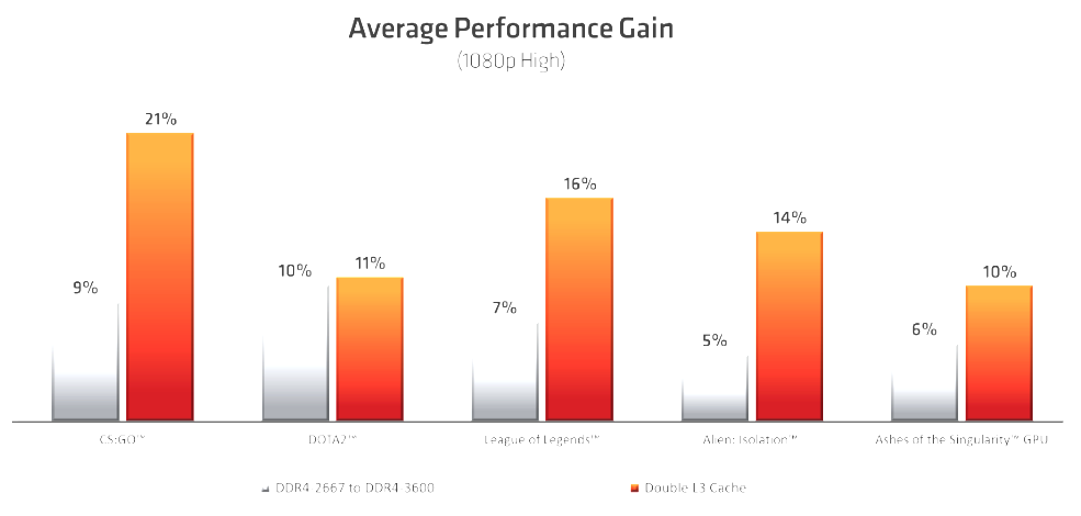
The chart above shows gains from memory clock speed increases as well as L3 cache increases. In general, games rarely benefited from increasing memory clock speeds and frankly, these numbers seem a bit high. That said, the Zen+ architecture does have a better memory controller with less memory latency. The AMD platforms have always been sensitive to memory latency, so it stands to reason that these gains are probably more from improvements in latency than outright clock speed. Of course, this is something I haven’t had the opportunity to test myself, so that’s speculative on my part. In any case, AMD’s data shows bigger gains from the larger L3 cache than it does memory clock speed increases. While I remain skeptical on the point concerning memory speed increases and gaming performance, I have seen the performance increase that comes with the L3 cache increase and other architectural changes. They are very real and help close that gap AMD has compared to Intel when it comes to gaming performance.
This is such a big deal for AMD that it’s marketing slides and future marketing material will refer to the L3 cache as “AMD GameCache.” It is important to understand that as you may see articles refer to L3 and GameCache interchangeably. Thus, to avoid confusion its important to note that they are the same thing.
Processor Topology
Another factor impacting gaming performance was the latency penalties incurred when crossing CCX complexes. We already talked about this as it relates to the Windows scheduler. In fact, AMD’s game mode which was accessible via Ryzen Master allowed the user to disable remote CCX complexes and reduce the CPU’s internal latency. This cost you half your cores. In the case of a Threadripper 2950X, you would turn your 16c/32t CPU into an 8c/16t CPU more in line with a Ryzen 2700X in terms of gaming performance. However, an 8c/16t CPU still housed two CCX complexes and thus, latency penalties still existed when crossing them. The new architectural layout of CCD’s containing CCX complexes and the centralized I/O die help to mitigate these issues.
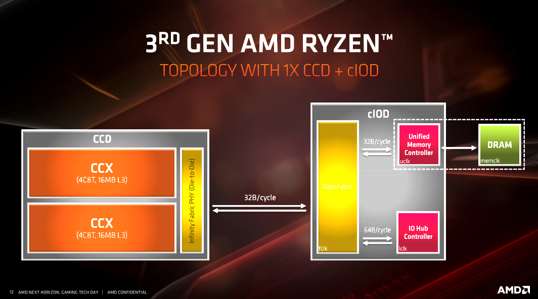
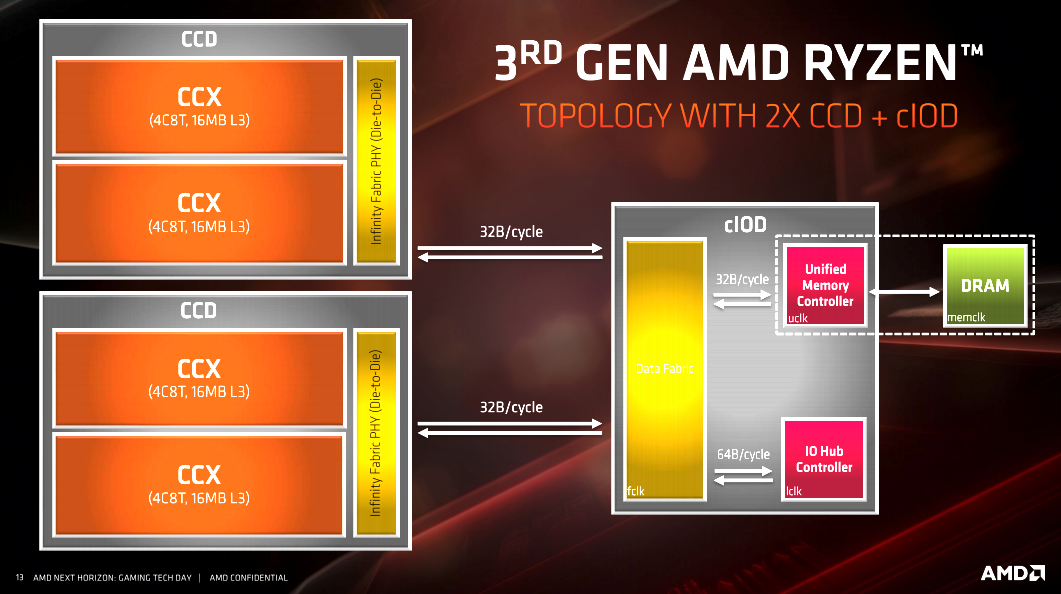
The above block diagrams show you the topology of both 8c/16t and the larger 12c/24t and 16c/32t 3rd generation Ryzen CPU’s. As you can see, all CCD’s and complexes within the CCD’s have equal access to the cIOD (I/O die) and other system resources via the Infinity Fabric.
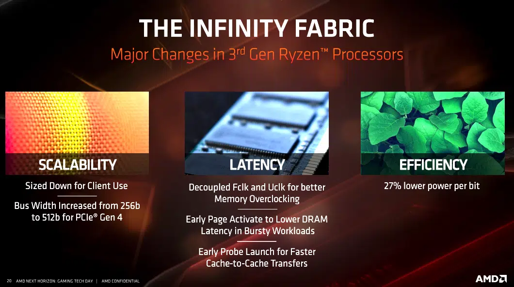
The Infinity Fabric is basically a proprietary, modular system interconnect which allows for data transmission across various linked components. It is utilized by both CPU’s and GPU’s. The bus was increased from 256b to 512b for PCI-Express Gen 4. As the slide shows, the Infinity Fabric clock or “fclk” and unified memory controller clock or “uclk” have been decoupled to allow for greater memory speeds. This is what I was referring to earlier when talking about memory overclocking beyond DDR4 3600MHz and 1:1:1 or 2:1 ratio between the memory clock, memory controller clock, and Infinity Fabric clocks. When in 2:1 mode, the Infinity Fabric is set at 1800MHz. This can also be adjusted in 33MHz increments.