Memory Support
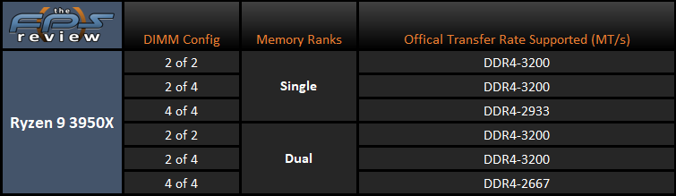
As you can see from the table below, for the most part, you can achieve memory speeds of at least 3200MHz officially using two DIMMs. Going to four modules reduces your speeds to DDR4 2933MHz using single ranked memory and 2667MHz using dual ranked modules. Of course, your mileage may vary. Some people have had greater success achieving higher clocks than others, but this is the official line from AMD. Walk outside the lines at the risk of disappointment. On that front, AMD’s Ryzen 3000 series is a bit strange as it relates to memory. I plan on doing an article about this at some point and have even acquired some modules to help me prove the point, but that’s a topic for another time.
In any case, AMD made it very clear in the press kits for the 3000 series launch that going beyond DDR4 3733MHz wasn’t a great idea as it forces the use of memory dividers between the Infinity Fabric clocks and the memory clocks rather than the usual 1:1 ratio. DDR4 3600MHz is suggested as the sweet spot for price and performance. Speeds of DDR4 3800MHz are certainly possible, but at a point of diminishing returns. Of course, AMD also added that eventually it may be possible to offset the performance impact if the RAM used has enough bandwidth to make up for it. Basically, going beyond 5,000MHz may be enough to make it worthwhile, but this isn’t something we’ve tested. To be frank, I’m not sure AMD has tested this either given how the statement was worded.
CPU Layout
For those who do not know, the CPU is compatible with existing socket AM4 motherboards. This includes some B350 motherboards, X370, B450, X470 and X570 motherboards. You will need a motherboard that can handle a CPU operating at over 200watts at times. Additionally, the CPU is comprised of three CCD’s or chiplets. Two of these contain the CCX complexes while the third is the I/O die. Each CCD or CCX complex has equal access to the I/O die. The CCD’s are 7nm while the IO die is 12nm. Each of the two CCD’s containing CCX complexes contain two CCX complexes each. This results in a total of 4 cores per CCX and two CCX’s per CCD. Two CCD’s equals 16 cores. The 3900X is laid out the same way, but only has 3 cores per CCX across two CCD’s for a total of 12.
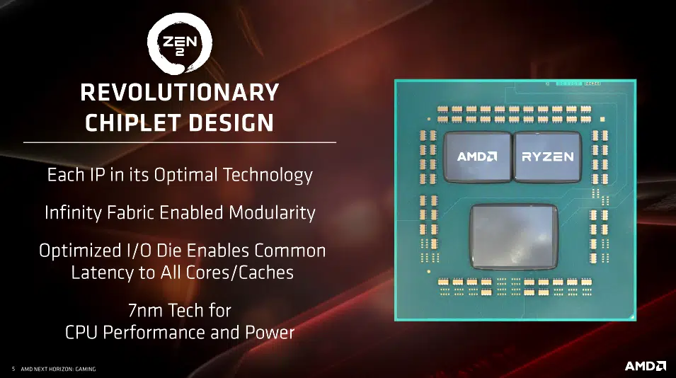
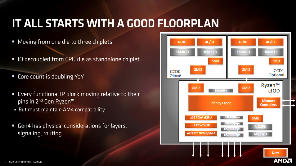
The above slides from AMD illustrate the architectural layout. The design is a modular one that has several advantages from a scaling and manufacturing perspective. The design also addresses several weaknesses in the previous iterations of the Zen microarchitectures. Again, I won’t get too deep into the weeds on this subject as we’ve covered it before. You can find that coverage here.